
Intel Xeon Processor Multiprocessor Platform Design Guide

83
Processor Power Distribution Guidelines
8.11 Validation Testing
The processor V
CCSENSE
and V
SSSENSE
pins should be routed to vias. The vias should be as close
to the socket pins as possible and should be connected with a low impedance trace. As these signals
provide measurement points to verify adherence to the processor's V
CC
specifications, the vias
need to be accessible to measurement equipment.
Intel recommends the following guideline when measuring the transients on the processor V
CC
.
The measurement should be done across the V
CC
and V
SS
pins on processor socket. Use an
oscilloscope with 100 MHz bandwidth, 1.5 pF maximum probe capacitance, and 1 mΩ minimum
impedance. The maximum length of ground wire on the probe should be less than 5 mm. Ensure
external noise from the system is not coupled in the scope probe. Some probes have a very
significant level of inherent noise. Attempt to minimize noise by investigating different probes.
Use a differential probe to make the voltage measurements. The bandwidth of the probe should be
no less than the oscilloscope. Ensure all connections from oscilloscope to motherboard pin are
good and have a very low contact resistance.
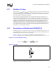
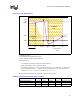
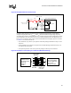
8.12 Generating and Distributing GTLREF[3:0]
GTLREF[3:0] are low current inputs (less than 15 µA each) to the differential receivers within each
of the components on the AGTL+ bus. A simple voltage divider can generate GTLREF[3:0]. The
GTLREF[3:0] inputs need to meet the 2% specification.
Equation 8-1 uses R
1
= 2 × R
2
to generate a GTLREF set at a nominal value of 2/3 V
CC
.
Figure 8-13 illustrates using 1% resistors to generate the GTLREF specification of 2/3 V
CC
± 2%.
Equation 8-1. Creating GTLREF of 2/3 V
CC
R
1
and R
2
should be small enough values that the current drawn by the GTLREF inputs (I
REF
) is
negligible versus the current caused by R
2
and R
1
.
Figure 8-13. GTLREF
CC
3
2
22
2
CC
21
1
CCREF
2
2
V
RR
R
V
RR
R
VV =
+×
×
×=
+
×=
R
2
V
V
CC
R
1
I
S
I
REF
SS
GTLREF