
Intel Xeon Processor Multiprocessor Platform Design Guide


47
System Bus Routing
The SM_TS_A[1:0] signals set the SMBus address for the thermal device on the processor. These
signals need to be set at power up with a unique address per bus. The SM_TS_A[1:0] can be set to
a logic high, a logic low, or a high impedance state giving nine possible combinations of addresses.
Refer to the section on SMBus Device Addressing in the datasheet for addressing details. The
SM_TS_A[1:0] signals do not have an internal pull down and thus need to be pulled to V
SS
or
SM_VCC with a 1 kΩ or smaller resistor. Leaving the pins floating achieves a high-Z state.
The SM_WP signal is a write protect signal for the memory device. Pulling this signal to SM_VCC
will enable write protection. SM_WP has an internal 10 kΩ pull-down.
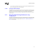
6.4.2.5 Topology 5: BR[3:0]# Signals
Since the Intel Xeon processor MP and Intel Xeon processor MP with up to 2-MB L3 cache on the
0.13 micron process does not have on-die termination on the BR[3:0]# signals, it is necessary to
terminate using discrete components on the motherboard. Connect the BR[3:0]# signals as in the
past by “swizzling” the lines between the processors as shown in Figure 6-12, below. The chipset
has on-die termination for BR0# and thus it is necessary to terminate only at the processor end. See
the routing guidelines below. For other routing guidelines such as trace spacing and layer
referencing follow the guidelines for common clock signals in Section 6.4.1.
NOTES:
1. .The maximum distance between one and only one set of agents may be up to 6.9 inches.
2. New designs are those platforms that only intend to support Intel Xeon processors MP with up to 2-MB L3
cache on the 0.13 micron process.
Supports Trace Zo
L1
Agent-to-agent
L2 (BR0#)
Agent-to-Chipset
L3
Agent-to-Rpu
stub
R
T
Existing
Designs
50
Ω 3.0 to 6.1 inches
1
Up to max total bus
length of 20.8 inches
1 inch max 41
Ω ± 5%
New
Designs
2
50 Ω 3.0 to 6.1 inches
1
Up to max total bus
length of 20.8 inches
1 inch max 50
Ω ± 5%
Figure 6-12. BR[3:0]# Connection for 4-Way Configuration
Chipset
Proc. 4 Proc. 3 Proc. 2 Proc. 1
Vcc
BR0
#
BR1
#
BR2
#
BR3
#
BR0
#
BR1
#
BR2
#
BR3
#
BR0
#
BR1
#
BR2
#
BR3
#
BR0
#
BR1
#
BR2
#
BR3
#
Vcc
BREQ0#
BREQ2#
BREQ1#
BREQ3#
R
T
R
T
L1 L3
L2
L3