
Intel Xeon Processor and Intel E7500/E7501Chipset Compatible Platform Design Guide


Intel
®
Xeon™ Processor and Intel
®
E7500/E7501 Chipset Compatible Platform Design Guide 179
Platform Power Delivery Guidelines
be in the open state whenever VCC_CPU is within its specified range. At power up, the PWRGD
signal must remain in the low-impedance state until the output voltage has stabilized within the
required tolerance.
The minimum voltage at which PWRGD is asserted should be the minimum VCC_CPU specified
in the Intel
®
Xeon™ Processor Datasheet, minus margin to prevent false deassertion, but at least
95% of (VID minus 125 mV). The maximum voltage at which PWRGD is asserted should be the
VID set-point voltage, plus margin to prevent false deassertion, but must be no greater than
(VID plus 250 mV).
This PWRGD should be capable of sinking up to 4 mA while maintaining a voltage of 0.4 V or
lower. When the output is in the open state, it should be capable of withstanding up to 5.5 V. Latch-
up or damage cannot occur if the pull-up voltage on the system board is present with no +12 V
input present. VR Power Good should remain low if the VR is disabled by the Output Enable
(OUTEN) pin.
11.2.3.3 Fault Protection
When looking for a VR solution, you can look for some fault protection features. The features help
the VR to prevent damage to itself and the circuits it powers. The VR should provide over-voltage
protection (OVP) by including a circuit, separate from the voltage sense path, capable of shutting
off the output drive when the output voltage rises beyond Vtrip. The power input (12 V) should be
protected with a fuse rated not greater than 30 A that sustains all operating and inrush conditions,
and that “blows” only for catastrophic failure of the VR. The VR should be capable of withstanding
a continuous, abnormally low resistance on the output without damage or over-stress to the unit. If
the VR goes into a shutdown state due to a fault condition on its output (not an internal failure), it
should return to normal operation after the fault has been removed, or after the fault has been
removed and power has been cycled off and on.
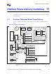
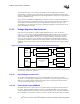
11.2.3.4 VID Routing and Enable Logic
Figure 11-4 shows the recommended implementation of logic for monitoring the VID pins of all
processors. This logic will determine that all of the installed processors are requesting the same
VCC. If mixed voltage processors are detected, the output enable signal (OUTEN) of all VRs must
be disabled. Note that if the middle processor is not installed, the VID[4:0] of that processor are all
high, and this should not cause disabling of the output of other VRs. The VID lines must be pulled
up internally in the VR.
Figure 11-4. VRM VID Routing
Power
Supply
Processor 1
VIDx[4:0]
OUTEN
Output Enable Logic
VCC_CPU
Processor
Voltage
Regulator
+12 V
Processor 0
VIDx[4:0]
Power OK