
ITP700 Debug Port Design Guide

R
ITP700 Debug Port Design Guide 13
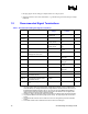
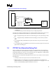
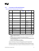
Figure 1. PWR Routing and Usage
1.5 K 1%
3.0 K 1%
Vterm
ITP 700
Debug Port
Pin PWR
Platform MB
Vpwr
Reset#
+
-
Vpwr
BPM[5:0]#/Reset#
Signals
Recovery
Point
+
-
+
-
.
.
BPM5#
BPM0#
BPM1#
NOTE: By varying the platform 1.5-K resistor, the recovery point could be increased or decreased.
1.3 ITP Signal Layout Guidelines
This section contains the layout guidelines for the debug port signals. Please refer to the
specification chapter for the debug port electrical and mechanical specifications. Routing to the
debug port of Signals BPM[5:0]# and RESET# must be shorter than 1.0 ns of electrical length
from the nearest system bus agent. Note that the <1.0 ns requirement applies only to the
BPM[5:0]# and RESET# trace segments between the debug port and the nearest system bus agent.
All other system bus trace segments must be routed according to the guidelines located in the
Platform Design Guides.
There are three signal groups within the debug port. Each group has a different set of layout
requirements:
• System - The system signal group indicates the access state of the entire system
• JTAG - The JTAG signal group consists of the five standard JTAG pins. The JTAG signals
are to be designed to run up to 16 MHz.
• Execution - The execution signal group contains the reset and run control signals used to
indicate operational conditions.
The following three subsections clarify the routing guidelines for each of these signal classes.
VTERM is the termination voltage of the system bus BPM[5:0]# and RESET# signals as defined
by the processor data sheet. VTAP refers to the pull-up voltage of the JTAG signals on the system
board. This pull-up voltage is chosen by the system designers to be consistent with the JTAG IO
buffer specs for the processor and the ITP. Information on input voltage specifications, drive
strength, and recommended termination values for the processor can be obtained from processor