
Intel Xeon Processor and Intel E7500/E7501Chipset Compatible Platform Design Guide


Layout Checklist
252 Intel
®
Xeon™ Processor and Intel
®
E7500/E7501 Chipset Compatible Platform Design Guide
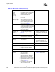
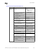
RAS_x#
CAS_x#
WE_x#
MA_x[12:0]
BA_x[1:0]
• Place termination resistor within 800 mills
from last DIMM connector. No more then
2 vias/layer transitions, not including
breakout and passive devices.
• Refer to Section 6.4.
CS_x[7:0]# • Place termination resistor within 1.5" from
the connector.
• Refer to Section 6.5.
CMDCLK_x[3:0]
CMDCLK_x[3:0]#
• Clock signals within a differential pair
must be matched to each other within
± 2 mils. These signals must be routed
5 on 7.5, and must be at least 20 mils
away from any other signal. Use exact
lengths as defined in Table 6-5.
• Refer to Section 6.3.
CKE_x • Route 40
Ω using a 7.5-mil wide trace.
The CKE signal must be length matched
to the clock signal at each DIMM within
2 inches. Place termination resistor within
800 mils from last DIMM connector. If
routing creates stubs, keep the stub
length less than 300 mils.
• Refer to Section 6.6.
RCVENIN_x#
RCVENOUT_x#
RCVEN_x
• Route 50
Ω using a 5-mil wide trace with
15-mil wide spacing. Use topology in
Figure 6-12.
• Refer to Section 6.7.1.
• RCVENIN_x# and RCVENOUT_x#
are on the E7500 chipset MCH and
RCVEN_x is on the E7501 chipset
MCH.
DDRCOMP_x • Route 15-mil wide trace with 20-mil wide
spacing. Place pull-up
resistor within
1 inch of the MCH.
• Refer to Section 6.7.2.
DDRCVOL_x
DDRCVOH_x
DDRCVO_x
• Route 15-mil wide trace with 20-mil wide
spacing. Place resistive network within
1 inch of the MCH.
• Refer to Section 6.7.4.
• DDRCVOL_x and DDRCVOH_x are
on the E7500 chipset MCH and
DDRCVO_x is on the E7501 chipset
MCH.
DDRVREF_x • Place a 0.1 µF capacitor next to each
MCH pin.
•
Decoupling • Spread termination decoupling capacitors
evenly around the termination plane.
• Spread 2.5 V decoupling capacitors
evenly around the DIMMs.
• Refer to Section 6.9.
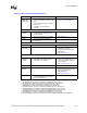
Hub Interfaces
General
Guidelines
• Hub interface spacing of 5 on 15 for data,
and 5 on 35 for strobes.
• Space signals out as much as possible on
breakout from the BGA.
• Hub interface data group signals are
routed on the same layer, transitioning
together if a layer change is required.
• Maximum length of 20" (stripline routing).
• Length match Hub Interface 2.0 strobes
within 1" from data. Length match
according to Figure 7-2.
• Hub Interface 1.5: Length match data
± 100 mils and strobes exactly.
• Refer to Section 7.2.1 and
Section 7.3.1of this document.
Table 14-3. MCH Layout Checklist (Sheet 2 of 3)
Checklist Items Recommendations Comments