
Intel Xeon Processor Multiprocessor Platform Design Guide

72
Processor Power Distribution Guidelines
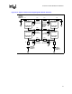
feasible. Possibly one or both ends of the capacitor can be connected directly to the pin of the
processor without the use of via. Even if simulation results look good, these practical suggestions
can be used to create an even better decoupling situation where they can be applied in layout.
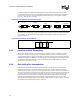
Figure 8-3 illustrates these concepts.
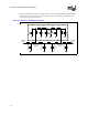
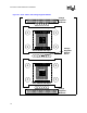
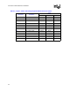
If polymer capacitors or large ceramics are being used, avoid the loss of the low ESL characteristic
by connecting via patterns as wide as the capacitor with multiple via holes per connection, as
shown in Figure 8-4.
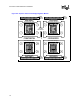
8.9.3 Location of Bulk Decoupling
The location of bulk capacitance is not as critical as the high-frequency decoupling since more
inductance is already expected for these components. However, to achieve better performance,
good placement of these components will affect the transient response of the system for the better,
as shown in simulation. In addition to the bulk capacitors on the voltage converter module, which
are electrically behind the inductance of the converter pins, several bulk capacitors need to be
placed close to the processor socket.
8.9.4 Decoupling Recommendation
Intel recommends that the baseboard design incorporates at least nine 560 µF OSCON bulk
capacitors and twenty 22 µF ceramic capacitors per processor. The bulk capacitors should be
placed, half on one side of the processor and half on the other as close to the processor package as
the keep-out zone allows. One quarter of the ceramic capacitors should be placed on one side of the
processor, one quarter on the other side, and half in the processor cavity using both sides of the
board. See Section 8.10 for placement options. Check with the voltage regulator designer for
optimal choice of bulk capacitors. Some very high switching regulators are better served by
replacing the OSCON bulk capacitors with additional high-frequency ceramics. Table 8-1 provides
the parameters for bulk and high-frequency capacitors.
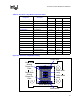
Figure 8-3. 1206 Capacitor Pad and Via Layouts
Bad
Vias
Very Good
Very Good
Pads
Capacitors
Good
Pin
Less Bad
Figure 8-4. Connections to Via Patterns
C