
Intel Xeon Processor Multiprocessor Platform Design Guide


28
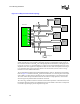
Clock Routing Guidelines
NOTES:
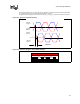
1. The skew budget includes clock driver output pair to output pair jitter (differential jitter), and skew, clock skew
due to interconnect process variation, and static skew due to layout differences between clocks to all bus
agents. This number does not include clock driver common mode (cycle to cycle) jitter or spread spectrum
clocking.
2. This number assumes all BCLK pairs are routed on the same signal layer.
3. Skew measured at the load between any two bus agents from pad to pad. Measured at the crossing point.
4. Edge to edge spacing between the two traces of any differential pair. Uniform spacing should be maintained
along the entire length of the trace.
5. Clock traces are routed in a differential configuration. Maintain the minimum recommended spacing between
the two traces of the pair. Do not exceed the maximum trace spacing, as this will degrade the noise rejection
of the network.
6. The differential impedance of each clock pair is approximately 2*Z single-ended*(1-2*Kb) where Kb is the
backwards crosstalk coefficient. For the recommended trace spacing, the Kb is very small and the effective
differential impedance is approximately equal to 2 times the single-ended impedance of each half of the pair.
7. The single ended impedance of both halves of a differential pair should be targeted to be of equal value. They
should have the same physical construction. If the BCLK traces vary within the tolerances specified, both
traces of a differential pair must vary equally.
8. Length compensation for the processor socket and package delay is added to chipset routing to match
electrical lengths between the chipset and the processor at die pad. Therefore, the motherboard trace length
for the chipset will be longer than that for the processor. Refer to the processor signal integrity models for
exact package compensation lengths.
9. Length of LT for one processor must match the LT of all other BCLK traces to other processors with specified
tolerance.
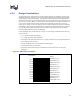
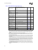
Serpentine spacing
Maintain a minimum S/h ratio of > 5/1
Keep parallel serpentine sections as short as
possible
Minimize 90 degree bends. Make 45 degree bends if
possible.
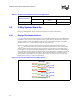
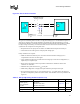
Figure 5-4
Motherboard Impedance –
Differential
100 Ω typical 6
Motherboard Impedance –
single ended
50 Ω ± 10% 7
Processor routing length –
L1: CK_WBY/CK_SKS to
R
S
0.5” max Figure 5-2 12
Processor routing length –
L4: R
S
/R
T
to Processor
0 – 12” Figure 5-2
Chipset routing length –
L1: CK_WBY/CK_SKS to
R
S
0.5” max Figure 5-2 12
Chipset routing length –
L4: R
S
/R
T
to Processor
0 – 12” Figure 5-2
L3: Stub length to R
T
Preferably without stubs
200 mils max from fork to R
T
pad.
Figure 5-2 12
L2: R
S
to fork to R
T
200 mils max from R
S
to fork to R
T
Figure 5-2 12
Processor to CS length
matching (LT)
0.13” ± 0.010”
Chipset LT must be 0.13” longer than Proc. LT.
Figure 5-2 8
Processor to Processor
length matching (LT)
± 10 mils Figure 5-2 9
BCLK0 – BCLK1 length
matching
±10 mils
R
S
Series termination value 33 Ω ± 5% Figure 5-2 10
R
T
Shunt termination value 49.9 Ω ±1% Figure 5-2 11
Table 5-1. BCLK[1:0]# Routing Guidelines (Sheet 2 of 2)