
Intel Xeon Processor and Intel E7500/E7501Chipset Compatible Platform Design Guide


Layout Checklist
246 Intel
®
Xeon™ Processor and Intel
®
E7500/E7501 Chipset Compatible Platform Design Guide
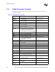
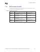
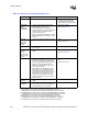
BPM[5:0]# • For all ITP interface signal
schematic, layout and routing
recommendations, refer to the
ITP700 Debug Port Design Guide.
FERR#/PBE#
IERR#
PROCHOT#
THERMTRIP#
• Connect to both processors and ICH3-S.
• Trace impedance = 50
Ω ± 10%.
• Route traces using 5/15-mil spacing.
• Try to keep signals on the same layer for the
whole bus, but not at expense of AGTL+
Source Synchronous I/O.
• Maximum agent to agent length is 10". Place
pull-up resistor within 3" of Processor 1 and
ICH3-S.
• Async GLT+ Output.
• Refer to Section 5.3.2.
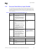
COMP[1:0]
ODTEN
SKTOCC#
TESTHI[6:0]
VID[4:0]
• There are no routing requirements for these
signals.
• Input.
• Refer to Section 5.3.
Reserved • Reserved signals must remain as a No
Connect (NC).
SM_ALERT#
SM_CLK
SM_DAT
SM_EP_A[2:0]
SM_TS_A[1:0]
SM_WP
• There are no routing requirements for these
signals.
•SMBus I/O.
• Refer to Section 5.5.1.
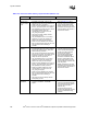
VCCA • To satisfy damping requirements, total series
resistance in the filter (from VCC_CPU to the
top plate of the capacitor) must be at least
0.35
Ω. It includes the minimum DCR of the
inductor, and any resistance (routing or
discrete components) between VCC_CPU
and capacitor top plate.
• The total maximum resistance cannot be
greater than 1.1
Ω as measured from VCC
(more specifically, the baseboard via that
connects the PLL filter to the VCC plane) to
the processor VCCA interposer pin. Also,
maximum trace resistance from the filter
capacitor to processor socket pin should be
less than 0.02
Ω.
• An isolated power for internal
PLL.
• Refer to Section 11.2.7.
VSSA
VCCIOPLL
• There are no routing requirements for these
signals.
• Refer to Section 11.2.7.
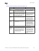
VCCSENSE
VSSSENSE
• Route traces using 5/15-mil spacing.
• Place via next to the processor socket’s pin
for measurement of VCC_CPU/VSS.
• Refer to Section 11.2.2.
NOTES:
1. A[35:3]# pins on the processor correspond to HA[35:3]# pins on the MCH.
2. ADSTB[1:0]# pins on the processor correspond to HADSTB[1:0]# pins on the MCH.
3. DSTBN[3:0]# pins on the processor correspond to HADSTBN[3:0]# pins on the MCH.
4. DSTBP[3:0]# pins on the processor correspond to HADSTBP[3:0]# pins on the MCH.
5. D[63:0]# pins on the processor correspond to HD[63:0]# pins on the MCH.
6. REQ[4:0]# pins on the processor correspond to HREQ[4:0]# pins on the MCH.
7. The RESET# pin on the processor corresponds to the CPURST# pin on the MCH.
8. The TRDY# pin on the processor corresponds to the HTRDY# pin on the MCH.
Table 14-1. Processor Layout Checklist (Sheet 2 of 2)
Checklist Items Recommendations Comments