
Intel Xeon Processor and Intel E7500/E7501Chipset Compatible Platform Design Guide
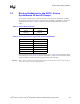

System Bus Routing Guidelines
66 Intel
®
Xeon™ Processor and Intel
®
E7500/E7501 Chipset Compatible Platform Design Guide
5.2 Routing Guidelines for Common Clock Signals
Table 5-5 lists the common clock signals.
NOTES:
1. RESET# has additional requirements in the ITP700 Debug Port Design Guide.
Route the common clock signals according to the processor system bus topology shown in
Figure 5-1. Routing guidelines for the common clock signal group are in Table 5-2. Route the
traces with at least 50% of the trace width directly over a reference plane. Common clock signals
may change layers.
5.2.1 Wired-OR Signals
The “wired-OR” signals are HIT#, HITM#, MCERR#, BINIT#, and BNR#. These signals differ
from the other system bus signals in that more than one agent can be driving the signal at the same
time. Intel recommends that special attention be given to the routing of these signals in adherence
to the layout guidelines presented in Table 5-2. Timing and signal integrity must be met for the
cases where one agent is driving, all agents are driving, and any combination of agents are driving.
The wired-OR signals should follow the same routing rules as the common clock signals. Intel
recommends that simulations for these signals be performed for each system.
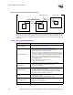
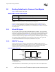
5.2.2 RESET# Topology
Since the processor does not contain on-die termination for the RESET# input signal, these
additional layout guidelines for the RESET# signal are required. The baseboard trace length from
Processor 0’s pin to the termination resistor should be 0 to 1 inch. Follow the same routing
guidelines given for common clock signals listed above in this same section.
NOTES:
1. Trace Z
0
= 50 Ω
2. Trace spacing = 10 mil
If ITP is implemented, see the ITP700 Debug Port Design Guide for the correct implementation.
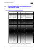
Table 5-5. AGTL+ Common Clock I/O Signals
Signal Types Signals
Input BPRI#, BR[3:1]#, DEFER#, RESET#
1
, RS[2:0]#, RSP#, TRDY#
I/O
ADS#, AP[1:0]#, BINIT#, BNR#, BR0#, DBSY#, DP[3:0]#, DRDY#, HIT#, HITM#, LOCK#,
MCERR#
Figure 5-2. RESET# Topology
MCH
Processor 1
Processor 0
VCC_CPU
0.1" - 1.0"
51 Ω ± 5%
3.0" - 7.0" 3.0" - 6.5"