
Intel Xeon Processor and Intel E7500/E7501Chipset Compatible Platform Design Guide

Platform Clock Routing Guidelines
50 Intel
®
Xeon™ Processor and Intel
®
E7500/E7501 Chipset Compatible Platform Design Guide
10.Length compensation for the processor socket and package delay is included in chipset routing to match
electrical lengths between the chipset and the processor from the die pad of each.
11.Minimize L1, L2 and L3 lengths. Long lengths on L2 and L3 degrade effectiveness of source termination and
contribute to ringback.
12.Do not change routed layers. The goal of constraining all bus clocks to one physical routing layer is to
minimize the impact on skew due to variations in Er and the impedance variations due to physical tolerances
of circuit board material.
13.Length of LT for one processor must match the LT of all other HOST_CLK traces to other processor with
specified tolerance.
14.If ITP is implemented, ITP HOST_CLK lengths need to be length matched to the processor HOST_CLK
lengths as specified in the
ITP700 Debug Port Design Guide.
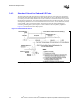
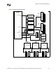
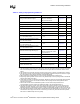
Figure 4-3. Clock Skew As Measured from Agent to Agent
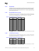
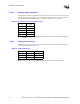
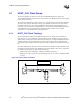
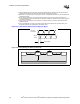
Figure 4-4. Trace Spacing for HOST_CLK Clocks
BCLK Slew
BCLK at
Processor
BCLK
at CS
h
W
S1S1
BCLK0 BCLK1
Ground Plane
S
W