
Intel Xeon Processor and Intel E7500/E7501Chipset Compatible Platform Design Guide

I/O Controller Hub 3 (Intel
®
ICH3-S)
150 Intel
®
Xeon™ Processor and Intel
®
E7500/E7501 Chipset Compatible Platform Design Guide
9.5.1 SMBus Design Considerations
There is not a single SMBus design solution that will work for all platforms. One must consider the
total bus capacitance and device capabilities when designing SMBus segments. Routing SMBus to
the PCI slots makes the design process even more challenging since they add so much capacitance
to the bus. This extra capacitance has a large affect on the bus time constant which in turn affects
the bus rise and fall times.
Regardless of the architecture used, there are some general design considerations.
• Device class (High/Low power). Most designs use primarily High Power Devices.
• Amount of VCC_SUSPEND current available (i.e., minimizing load of VCC_SUSPEND).
• The pull-up resistor size for the SMBus data and clock signals is dependent on the bus load
(this includes all device leakage currents). Generally the SMBus device that can sink the least
amount of current is the limiting agent on how small the resistor can be. The pull-up resistor
can not be made so large that the bus time constant (Resistance X Capacitance) does not meet
the SMBus rise and time specification.
• The maximum bus capacitance that a physical segment can reach is 400 pF.
• The ICH3-S does not run SMBus cycles while in S5.
• SMBus devices that can operate in S5 must be powered by the VCC_SUSPEND supply.
• If SMBus is connected to PCI it must be connected to all PCI slots.
• It is recommended that I
2
C devices be powered by the 1.8 V supply. During an SMBus
transaction in which the device is sending information to the ICH3-S, the device may not
release the SMBus if the ICH3-S receives an asynchronous reset. 1.8 V is used to allow BIOS
to reset the device if necessary. SMBus 2.0-compliant devices have a timeout capability which
makes them insusceptible to this I
2
C issue, allowing flexibility in choosing a voltage supply.
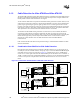
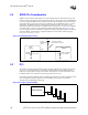
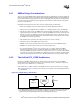
9.5.2 The Unified VCC_CORE Architecture
Designing an SMBus using the ICH3-S is based on the power supply source for the SMBus
microcontrollers. For the platform, all devices are powered by VCC3_3; therefore, the preferred
design choice is the unified VCC3_3 architecture.
In the unified VCC_CORE architecture, all SMBus devices are powered by the VCC3_3 supply.
This architecture in Figure 9-7 allows none of the devices to operate in S5, minimizing the load on
3.3 V SUSPEND.
NOTES:
1. The SMBus device must be back-drive safe while its supply (VCC3_3) is off and 3.3 V SUS is still powered.
2. In suspended modes where VCC3_3 is OFF and 3.3 V SUS is on, the VCC3_3 node will be very near
ground. In this case, the input leakage of the ICH3-S will be approximately 10 µA.
Figure 9-7. Unified VCC3_3 Architecture
Intel
®
ICH3-S
3.3 VSUS
SMBus
Devices
VCC_3.3
VCC_3.3
SMBus
8.2 kΩ