
Voltage Regulator Module (VRM) 10.2L Design Guidelines


VRM – Mechanical Guidelines
28 Voltage Regulator Module (VRM) 10.2L Design Guidelines
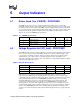
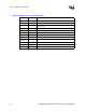
Table 7-2. VRM 10.2 Connector Pin Descriptions
Name Type Description
Load Current Output Analog signal representing the output load current
OUTEN Input Output enable
Vcc_PWRGD Output Output signal indicating that the output voltage of the VRM is in the
specified range
VID [5:0] Input Voltage ID pins used to specify the VRM output voltage
VIN+ Power VRM Input Voltage
VIN− Ground VRM Input Ground
VO+ Power VRM Output Voltage
VO− Ground VRM Output Ground
VO_SEN+
VO_SEN–
Input Output voltage sense pins
VR_hot# Output Indicates to the system that a thermal event has been detected in the VR
VRM_pres# Output Indicates to the system that a VRM is plugged into the socket
LL0, LL1 Input Used to configure VR load line value