
Intel Xeon Processor Multiprocessor Platform Design Guide

96
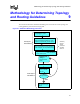
Methodology for Determining Topology and Routing Guidelines
9.1.2.1 Setup Margin
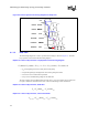
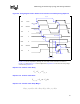
Figure 9-5 shows the setup timing diagram that was used to develop the final timing equations for
the setup margin.
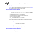
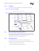
Equation 9-9. Common Clock Loop Equation
• T
cycle
is the cycle time
• T
drv_clk
(A)[(B)] is the delay of the clock buffer circuit connected to device A [B]
• T
prop_clk
(A)[(B)] is the delay of the interconnect between the clock buffer and device A [B]
• T
drv
is the delay of the output buffer for the data signal on device A (TCO)
• T
PROP
is the interconnect delay between device A and B
• T
setup
is the setup time required by the buffer
• T
jitter
is the clock cycle-to-cycle jitter
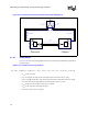
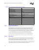
Figure 9-4. Circuit Used to Develop the Common Clock Timing Equations
CLK
D
Q
CLK
T
T
flight
T
setup
D
Q
CLK
AB
T (A) T
prop_clk
(B)
T
drv_clk
(B)T (A)
F
R
O
M
C
O
R
E
TO
C
O
R
E
Processor Chipset
drv
prop_clk
drv_clk
0)()()()(
__arg__
=−−−−−−−++ ATATTTTTTBTBTT
clkdrvclkpropdrvpropinmsetupjitterclkpropclkdrvcyvle