
Intel Xeon Processor and Intel E7500/E7501Chipset Compatible Platform Design Guide

Intel
®
Xeon™ Processor and Intel
®
E7500/E7501 Chipset Compatible Platform Design Guide 55
Platform Clock Routing Guidelines
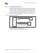
4.3 CLK33_ICH3-S Clock
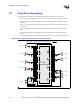
In the CLK33_ICH3-S case, the driver is the clock synthesizer PCIF 33 MHz clock output buffer,
and the receiver is the PCICLK 33 MHz clock input buffer at the ICH3-S. Care must be taken to
length match this 33 MHz clock with the ICH3-S 66 MHz clock.
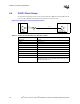
Figure 4-10. Topology for CLK33_ICH3-S
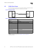
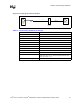
Table 4-5. CLK33_ICH3-S Routing Guidelines
Parameter Routing Guidelines
Clock Group CLK33_ICH3-S
Topology Point-to-Point
Reference Plane Ground referenced (contiguous over entire length)
Characteristic Trace Impedance (Z
0
) 50 Ω ± 10%
Trace Width 5 mils
Trace Spacing 25 mils
Trace Length – L1 0.00” – 0.50”
Trace Length – L2 3.00” – 9.0”
Resistor R1 = 33
Ω ± 5%
Skew Requirements Must be matched to ± 100 mils of CLK66
R1
L1
L2
Intel
®
ICH3-S
CK408
PCIF
PCICLK