
Intel Xeon Processor and Intel E7500/E7501Chipset Compatible Platform Design Guide


Intel
®
Xeon™ Processor and Intel
®
E7500/E7501 Chipset Compatible Platform Design Guide 253
Layout Checklist
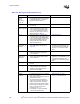
HIRCOMP_x
HIVREF_[D:A]
HISWNG_[D:A]
• RCOMP, VSWING, VREF resistor
networks are less than 1” away from the
MCH.
• VSWING, VREF trace width is greater
than 15 mils.
• HIRCOMP_x must have a 50
Ω
impedance.
• Refer to Section 7.2.2, Section 7.2.3,
Section 7.3.2, and Section 7.3.3.
Clocks, Reset, Miscellaneous Signals
HCLKINP
HLCKINN
• HCLKs should be length matched to all
processors BCLKs. See Table 4-3 for
routing guidelines.
• Refer to Section 4.1.
CLK66 • Place series resistor close to CK408B. • Refer to Section 4.2.
RSTIN# • Connect to PCIRST# output of the
Intel
®
ICH3-S.
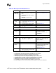
Miscellaneous Signals
XORMODE#
HXRCOMP
HYRCOMP
• This signal is used to calibrate the
Host AGTL+ I/O buffers
characteristics to specific board
characteristic.
• Refer to Section 5.3.3.
Voltage References – Power Planes
HDVREF[3:0]
HAVREF[1:0]
HCCVREF
• Use one dedicated voltage divider for all
these signals. Decouple the voltage
divider with a 1 µF capacitor.
• To provide constant and clean power
delivery to the data, address, and
common clock signals of the host
AGTL+ interface.
• Refer to Section 11.2.10.
DDRVREF_x[5:0] • Refer to Section 6.7.
HXSWING
HYSWING
• The HXSWING and HYSWING
inputs of MCH are used to provide
reference voltage for the
compensation logic.
• Refer to Section 5.3.3.
VCCA • High-frequency decoupling for VCCA
planes is located as close as possible to
the associated MCH ball.
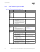
NOTES:
1. The BREQ0# pin on the MCH corresponds to the BR0# pin on the processor.
2. The CPURST# pin on the MCH corresponds to the RESET# pin on the processor.
3. HA[35:3]# pins on the MCH correspond to A[35:3]# pins on the processor.
4. HD[63:0]# pins on the MCH correspond to D[63:0]# pins on the processor.
5. HADSTB[1:0]# pins on the MCH correspond to ADSTB[1:0]# pins on the processor.
6. HADSTBN[3:0]# pins on the MCH correspond to DSTBN[3:0]# pins on the processor.
7. HADSTBP[3:0]# pins on the MCH correspond to DSTBP[3:0]# pins on the processor.
8. HREQ[4:0]# pins on the MCH correspond to REQ[4:0]# pins on the processor.
9. The HTRDY# pin on the MCH corresponds to the TRDY# pin on the processor.
10.The MCH XERR# pin can be connected to the processor IERR# pin or the processor MCERR# pin.
Table 14-3. MCH Layout Checklist (Sheet 3 of 3)
Checklist Items Recommendations Comments