
Intel Xeon Processor Multiprocessor Platform Design Guide


27
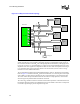
Clock Routing Guidelines
The goal of constraining all bus clocks to one physical routing layer is to minimize the impact on
skew due to variations in Er and the impedance variations due to physical tolerances of circuit
board material. Routing on internal layers provides the least amount of Er and impedance variation.
If a layer change is necessary, increase the amounts of interconnect skew used in the timing
equations for the component receiving that clock.
• Requirement: Do not split up the two halves of a differential clock pair between layers.
• Goal: Route clocks to all agents on same physical routing layer.
If layer transitions are required:
• Make sure that skew induced by the vias used to transition between routing layers is
compensated in the traces to other agents.
• Layer transitions should only be made between routing layers of the same configuration, i.e.,
stripline layer to stripline layer.
• Keep routes to all agents as short as possible to minimize the cumulative effects of Er
variations on clock skew.
• Maintain return path referenced to V
SS
for the pair.
• Match delays (flight time or length) from pad of CK00 to pad of processor input.
• If a layer change must occur, use vias connecting the V
CC_CPU
planes and/or V
SS
planes to
provide a low impedance path for the return current. Vias should be as close as possible to the
signal via.
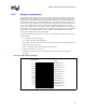
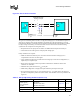
Figure 5-2. Source Shunt Termination
L3
L3
L4
L4
R T
CPU or
CS
CLOCK
DRIVER
L1
L1'
RS
Differential Bus Clock
Topology. (one pair
h)
LT =
L1+L2+L4
Cpu
or CS
p
in
Ck00
pin
L2’
L2
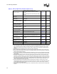
Table 5-1. BCLK[1:0]# Routing Guidelines (Sheet 1 of 2)
Layout Guideline Value Figures Notes
BCLK Skew assumptions
(between agents)
4-way configuration
CK_WBY
200 pS total
100 pS for Clock driver
100 pS for interconnect
Figure 5-3 1, 2, 3
Differential pair spacing 4 x W min. to 5 x W max. Figure 5-4 4, 5
Spacing to other traces 5 x W min. Figure 5-4