
Voltage Regulator Module (VRM) 10.2L Design Guidelines

Voltage Regulator Module (VRM) 10.2L Design Guidelines 9
2 Output Voltage Requirements
2.1 Voltage and Current - REQUIRED
There will be independent selectable voltage identification (VID) codes for the core voltage
regulator. The regulator’s 6-bit code (VID) will be provided by the processor to the VRM, which
will determine a reference output voltage, as described in Section 3.2. Section 2.2 and Section 2.3
specify deviations from the VID reference voltage.
The load line tolerance in Section 2.2 shows the relationship between Vcc and Icc for the
processor.
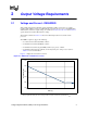
The VRM is required to support the following:
• A continuous load current (IccTDC) of 105 A.
• A maximum load current (IccMAX) of 120 A.
• A maximum load current step (IccSTEP), within a 1 µs period, of 100 A.
• A maximum current slew rate (dIcc/dt) of 930 A/µs at the pins of the processor (refer to
Table 2-2 for more information).
Figure 2-1 displays the load current over time.
NOTE:
1. Voltage regulator thermal protection circuitry should not trip for load currents greater than Icc
TDC.
Figure 2-1. VRM 10.2L Load Current vs. Time
100
105
110
115
120
125
0.01 0.1 1 10 100 1000
Time (s)
Load Current (A)