
ITP700 Debug Port Design Guide

R
ITP700 Debug Port Design Guide 39
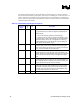
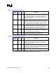
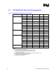
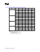
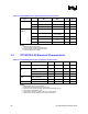
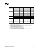
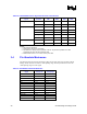
Table 21. ITP700 DPA JTAG Signal AC Electrical Characteristics
Signal Parameter Min Max Unit Note
Setup 5 ns 1
Hold 0.5 ns 1
TDO
Rise/Fall Time 15 ns 2
Rise/Fall Time 9 13 ns 2, 3
Period 58 ns 4
Time High 25 ns 5
TCK
Time Low 25 ns 5
Rise/Fall Time 7 16 ns 2, 6 TMS
Clock to Out -5 0 ns 7
Rise Time 0.5 2.0 ns 2, 8
Fall Time 0.5 2.0 ns 2, 8
TDI
Clock to Out -8 0 ns 7
TRST# Assert Time 300 ns
NOTES:
1. With respect to rising edge of FBO at the debug port using 50% of transition for both signals.
2. Measured from 20% to 80% of transition.
3. As measured into a 27 Ω and 35pF load to GND.
4. Measured from 50% of rising edge to 50% of next rising edge. This specification is valid for
asynchronous and synchronous operation.
5. Measured from 50% of first edge to 50% of second edge.
6. As measured into a 39 Ω load to VTAP and 35pF to GND.
7. With respect to falling edge of TCK at the debug port using 50% of transition for both signals.
8. As measured into a 1500 Ω load to VTAP and 10pF to GND.