
Intel Xeon Processor Multiprocessor Platform Design Guide

73
Processor Power Distribution Guidelines
8.10 Component Placement and Modeling
Intel recommends using simulation to design and verify Intel Xeon processor MP and Intel Xeon
processor MP with up to 2-MB L3 cache on the 0.13 micron process-based systems. The models in
the following sections can be used to piece together a complete base board spice circuit.
The maximum distance between each processor and its voltage regulator module should not be
greater than 1.5 inches. To be more specific, the distance between the facing edges of the VRM
connector and the socket should be no more than 0.5 inch. The bulk capacitors can be placed close
to and the high-frequency capacitors should be placed next to the processors. Distribute the bulk
and high-frequency capacitors equally on both sides of the socket where the power/ground pins are
located (the east and west side).
Intel Xeon processor MP and Intel Xeon processor MP with up to 2-MB L3 cache on the 0.13
micron process sockets have 603-pins with 50-mil pitch. The routing of the signals, power and
ground pins will require creation of lots of vias. These vias cause a “Swiss cheese” effect in the
power and ground planes beneath the processor resulting in increased inductance of these planes. It
is recommended to place as many high-frequency capacitors as possible inside the cut out of the
processor socket. The remaining high-frequency capacitors should be placed next to the processor,
specifically the power/ground pins.
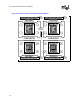
Processors should be placed with respect to the voltage regulator modules and bulk decoupling
capacitors such that current to one processor does not flow in the same path as that of any other
processor.
8.10.1 Component Models
Acquire component models from their respective manufacturers. Intel cannot guarantee the
specifications of another manufacturer's components. This section contains some of the models
developed by Intel for internal simulations.
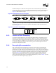
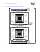
8.10.2 Processor Socket-Package Lump Model
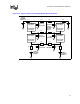
Figure 8-5 shows the lump electrical model for the high-frequency baseboard capacitors, the
processor socket, and the processor package. Figure 8-6 shows a physical pictorial of the model.
This model serves as a sub-circuit for the following baseboard models. Table 8-2 lists the model's
component values. L2 and L6 refer to the inductance and resistance of the power plane next to the
processor socket area, i.e., “before Swiss cheese” area. L3 and L5 refer to the inductance and
resistance of the power plane within the processor socket area, i.e., “after Swiss cheese” area. The
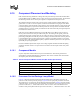
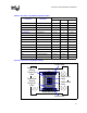
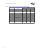
Table 8-1. Various Component Models Used at Intel (Not Vendor Specifications)
Component of Simulation ESR (Ω)ESL (nH)
0.1 µF Ceramic 0603 package 0.006 0.63
1
µF Ceramic 0805 package 0.080 0.702
10.0
µF Ceramic 1206 package 0.010 0.880
22.0
µF Ceramic 1210 package 0.010 1.1
560
µF OSCONS 0.012 3.1