
Intel Xeon Processor Multiprocessor Platform Design Guide


115
Design Checklist
Design Checklist 11
Use the following checklists as a final check to ensure the motherboard incorporates solid design
practices. These lists are only a reference. For correct operation, all of the design guidelines within
this document must be followed.
The following tables are quick checklists for platform design. They are created to provide a
reminder for key design points or easily forgotten items. These lists are by no means
comprehensive, nor do they attempt to explain routing and layout rules. Please refer to the sections
provided for detailed instructions.
11.1 Processor Family Connection Checklist
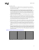
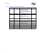
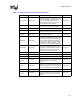
Table 11-1. Processor Connection Checklist (Sheet 1 of 5)
Processor Pin Signal Type Pin Connection Section No.
A[35:3]#
Source synch
AGTL+
Connect to all system bus agents. Balance
signal lengths within strobe group.
Section 6.4.1
A20M# Asynch GTL+
Connect to chipset or transition logic. Requires
300
Ω pull-up.
Section 6.4.2
ADS# Common Clock Connect to all system bus agents. Section 6.4.1
ADSTB[1:0]
Source synch
AGTL+
Connect to all system bus agents. Balance
signal lengths within strobe group. Maintain
25 mil spacing from all other signals.
Section 6.4.1
AP[1:0]# Common Clock Connect to all system bus agents. Section 6.4.1
BCLK[1:0] Bus Clock
Connect the clock driver. BCLK's to all
processors should be length matched, and the
BCLK to the chipset should be offset
accordingly. Maintain proper spacing.
Section 5.1.1
BINIT# Common Clock
Connect to all system bus agents, and the
chipset if supported. Wired-OR signal.
All wired-OR signals should have 143
Ω
termination to VCC_CPU at the middle agents
(see Figure 6-7). The termination should be
located as close as possible to the processor
pins with no stubs.
Section 6.4.1