
Intel Xeon Processor Multiprocessor Platform Design Guide


26
Clock Routing Guidelines
The CK00 clock driver differential bus output structure is a “Current Mode Current Steering”
output which develops a clock signal by alternately steering a programmable constant current to
the external termination resistors R
T
. The resulting amplitude is determined by multiplying IOUT
by R
T
. The current I
OUT
is programmable by a resistor and an internal multiplication factor so the
amplitude of the clock signal can be adjusted for different values of R
T
for impedance matching or
to accommodate future load requirements. Refer to the CK00 Clock Synthesizer/Driver Design
Guidelines for more detailed information.
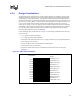
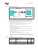
The recommended termination for the CK00 differential bus clock is a “Shunt Source termination”.
Refer to Figure 5-2. Parallel resistors R
T
perform a dual function, one converting the current output
of the CK00 to a voltage and two matching the driver output impedance to the transmission line.
The series resistors R
S
provide Isolation from the clock driver's output parasitics, which would
otherwise appear in parallel with the termination resistor R
T
.
The value of R
T
should be selected to match the characteristic impedance of the motherboard and
R
S
should be between 20 Ω and 33 Ω. Simulations have shown that R
S
values above 33 Ω provide
no benefit to signal integrity, but do degrade the edge rate.
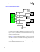
Figure 5-1. 4-Way Processor BCLK Topology
Processor
1
Processor
2
Processor
3
Chipset
Processor
0
CKx_WBY
Rs
Rs
RT
RT
Rs
Rs
RT
R
T
Rs
Rs
R
T
R
T
Rs
Rs
R
T
R
T
R
s
R
s
R
T
Rs
Rs
RT
RT
Clock Driver
Debug port
R
T