
ITP700 Debug Port Design Guide


R
66 ITP700 Debug Port Design Guide
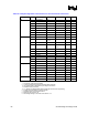
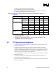
Table 35. ITP System Signal DC Characteristics for the Intel
®
Itanium
®
2 Processor
Signal DPA Type Min Max Unit Note
V
OH
ITP700DPA 1.00 V 1
LVDPA 0.9*VTAP VTAP+0.250 V 1, 9.
V
OL
ITP700DPA 0.40 V 1
LVDPA 0 0.1*VTAP V 1
I
OH
ITP700DPA -5 mA
LVDPA -8 mA
I
OL
ITP700DPA 5 mA
FBI
LVDPA 16 mA
V
IH
ITP700DPA 0.90 1.70 V
LVDPA 0.5*VTAP
+0.150
V
V
IL
ITP700DPA 0.00 0.55 V
LVDPA 0.5*VTAP -
0.150
V
I
IH
ITP700DPA -150 µA
LVDPA -100 µA
I
IL
ITP700DPA 300 µA
FBO
LVDPA 100 µA
V
IH
0.30 2.80 V 2
V
IL
0.10 V 3
PWR
R
PWR
2.95 3.05 kΩ 4
V
IH
1.70 V
V
IL
0.10 V
V
PTP
300 mV 5
I
IH
-1 mA
I
IL
300 µA
BCLK(p/n)
C
IN
10 pF 6
R
DBX
6 Ω 7 DBA#, DBR#
I
DBX
120 mA 8
NOTES:
1. At maximum output current specified.
2. V
IH
Max represents the maximum functional voltage of this pin.
3. ITP outputs will be tri-stated when input voltage is sensed low.
4. Resistance from pin to GND.
5. V
PTP
defined as voltage between both the high and low sides of the signal swing.
6. Including capacitive effects of mated connector.
7. Resistance from pin to GND when active.
8. Maximum sink current of ITP.
9. FBI Voltage tracking for VOH has a lower limit of 1.2 V.