
Intel Xeon Processor and Intel E7500/E7501Chipset Compatible Platform Design Guide

Intel
®
Xeon™ Processor and Intel
®
E7500/E7501 Chipset Compatible Platform Design Guide 231
Schematic Checklist
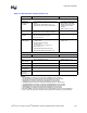
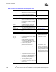
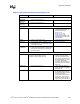
Voltage References – Power Planes
HDVREF[3:0]
HAVREF[1:0]
HCCVREF
• Use one dedicated voltage divider for all these
signals.
• Decouple the voltage divider with a 1 µF
capacitor and use a 220 pF at the MCH pins.
• To provide constant and clean
power delivery to the data,
address and common clock
signals of the host AGTL+
interface.
• Refer to Section 11.2.10.
DDRVREF_x[5:0] • Decouple each signal to ground with 0.1 µF
parallel capacitor at each DIMM and MCH pin.
• Refer to Section 6.7.3.
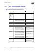
HXSWING
HYSWING
• 150
Ω ± 1% pull-down to ground
• 301
Ω ± 1% pull-up to VCC_CPU
• C1 = C2 = 0.01 µF
• Refer to Section 5.3.3.
HISWNG_[D:A],
HIVREF_[D:A]
• MCH Hub reference swing voltage
= 0.800 V ± 5%.
• MCH Hub reference voltage
= 0.350 V ± 5%.
• R1 = 392
Ω ± 1%, R2 = 499 Ω ± 1%,
R3 = 453
Ω ±1%.
• Decouple the MCH pin with a 0.01 µF.
• Decouple the network nodes with a 0.1 µF
• Refer to Section 7.2.2 and
Section 7.3.2.
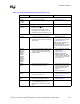
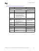
Voltage Sequencing Requirement
1.2 V and 2.5 V • 1.2 V must rise with or before 2.5 V. • Refer to Section 11.3.6.
Decoupling Requirements
1.25 V
(DDR VTERM)
• Two 0.1 µF and two 0.01 µF. • Refer to Section 11.3.1
VCC_CPU • Fourteen 0.1 µF • Refer to Section 11.3.2
2.5 V • Twenty-three 0.1 µF • Refer to Section 11.3.3
1.2 V
(Hub Interface)
• Four 0.1 µF • Refer to Section 11.3.4
VCCA1_2
VCCAHI1_2
VCCACPU_1.2
• RLC network • Refer to Section 11.3.5
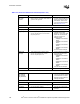
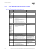
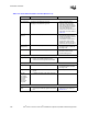
NOTES:
1. The BREQ0# pin on the MCH corresponds to the BR0# pin on the processor.
2. The CPURST# pin on the MCH corresponds to the RESET# pin on the processor.
3. HA[35:3]# pins on the MCH correspond to A[35:3]# pins on the processor.
4. HD[63:0]# pins on the MCH correspond to D[63:0]# pins on the processor.
5. HADSTB[1:0]# pins on the MCH correspond to ADSTB[1:0]# pins on the processor.
6. HADSTBN[3:0]# pins on the MCH correspond to DSTBN[3:0]# pins on the processor.
7. HADSTBP[3:0]# pins on the MCH correspond to DSTBP[3:0]# pins on the processor.
8. HREQ[4:0]# pins on the MCH correspond to REQ[4:0]# pins on the processor.
9. The HTRDY# pin on the MCH corresponds to the TRDY# pin on the processor.
10.The MCH XERR# pin can be connected to the processor IERR# pin or the processor MCERR# pin.
11.In HI1.0 mode, HI_STBF and HI_STBS used to be referred as HI_STB# and HI_STB respectively.
Table 13-2. MCH Schematic Checklist (Sheet 3 of 3)
Checklist Items Recommendations Comments