
Intel Xeon Processor and Intel E7500/E7501Chipset Compatible Platform Design Guide

High-Speed Design Concerns
218 Intel
®
Xeon™ Processor and Intel
®
E7500/E7501 Chipset Compatible Platform Design Guide
12.5.5 Bus Length Tuning Methodology
Many buses, such as memory and processor system bus, require length tuning a group of signals. A
common way to do this is by routing the bus first to determine what the approximate length range
is. Then, you can pick an arbitrary signal. Sometimes this signal may be the most difficult to route
or adjust to tune. Using the PCB trace length for this signal, you can determine the solution space
for the remainder of the signals and strobes in the group.
Intel commonly provides a length tuning calculator spreadsheet. This calculator uses a “seed
value.” This is the PCB length of an arbitrary signal, typically the signal with the shortest PCB
length. Then, the calculator uses all the routing parameters specified in the Platform Design Guide
(minimum and maximum lengths, tolerances, signal groups, etc.) to determine the solution space
for the bus in question.
12.6 Processor Bus Tuning
Routing the processor system bus requires length matching within source synchronous groups. A
major difference between the processor system bus and other source synchronous buses is the
loading effects from the middle socket processor. As a result, pure propagation-based length
matching cannot be used. Instead, length matching is based on both propagation and additional
signal integrity factors to account for the strobe-to-signal skew effects from the middle socket
processor. These two factors are described in the next two sections, followed by a routing example
in the last section.
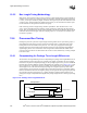
12.6.1 Compensating for Package Trace Length Differences
The first factor in length matching involves compensating for package trace length differences for
signals within the same strobe group. The “package trace length” is defined as the trace segment
between the die pad and component package pin. The package lengths on the processor and MCH
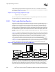
introduce skew between different signals as illustrated in the example given in Figure 12-13. Note
that “Component A” represents a processor or MCH. The example uses a strobe and data signal,
which happen to have the shortest and longest package trace lengths respectively. Each of the
signals will have varying amounts of package skew. The amount of skew for a particular signal is
based on the difference between that signal’s package trace length and the longest signal’s package
trace length in the same signal group. E.g., signals with shorter package length will have more
package trace length compensation than signals with package lengths closer to the longest package
trace.
Figure 12-13. Package Trace Length Differences
Longest Package Trace
Shortest Package Trace
Die Pad
Die Pad
Component A
Strobe Signal
Data Signal
Delta
Component Pin
PLC
Delta