
ITP700 Debug Port Design Guide


R
70 ITP700 Debug Port Design Guide
5. Measured from 50% of first edge to 50% of second edge.
6. As measured into a 39 Ω load to VTAP and 35 pF to GND.
7. With respect to falling edge of TCK at the debug port using 50% of transition for both signals.
8. As measured into a 1500 Ω load to VTAP and 10 pF to GND.
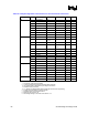
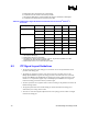
Table 40. ITP Execution Signal AC Electrical Characteristics for the Intel
®
Itanium
®
2
Processor
Signal Parameter Min Max Unit Note
Setup 400 ps 1 BPM[5:0]#, RESET
Hold 200 ps 1
Rise Time 5 ns 2
Fall Time 5 ns 2
Period 5 15 ns 3
Time High 2.2 ns
BCLK(p/n)
Time Low 2.2 ns
Rise Time 1 4 ns 2, 4 BPM5DR#
Fall Time 8 15 ns 2, 4
NOTES:
1. With respect to BCLK(p/n).
2. Measured from 20% to 80% of transition.
3. Specification for valid synchronous operation of the ITP. Asynchronous operation has no Max
specification but shares the Min specification listed.
4. Measured into a load to 1.5 V of 50 Ω and 35 pF to GND.
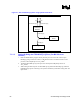
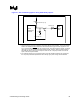
8.2 ITP Signal Layout Guidelines
• The physical placement of the debug port is critical for the correct implementation of all
processor node debug ports.
• The debug port should be treated as a part of the processor group with respect to the
BPM[5:0]# and RESET# signals. The debug port must be located within 1.0ns (electrical
length) of the BPM[5:0]# and RESET# pins and all next-nearest system bus agent(s). Note
that the <1.0 ns requirement applies only to the BPM[5:0]# and RESET# trace segments
between the debug port and the nearest system bus agent.
• All other system bus trace segments must be routed according to the guidelines located in the
Platform Design Guides.
• The physical placement of I/O domain debug port and the miscellaneous debug port is
determined by the routing rules for TCK.
• All receivers of the TCK signal (implemented in a star topology) must be within 2 ns flight
time from the debug port.