
ITP700 Debug Port Design Guide

R
14 ITP700 Debug Port Design Guide
datasheets. VTAP should be used for the pull-up resistors on all JTAG signals in the scan chain
that operates directly from the ITP. If a bus translator is used to translate an ITP scan chain to a
higher voltage, VTAP on the opposite side of the translator from the ITP shall change as well.
Note: All termination locations indicated are referenced to the target system.
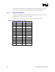
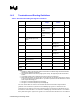
1.3.1 System Signal Layout Guidelines
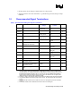
Table 2. System Signal Layout Guidelines
Debug Port Signal Layout Guideline
PWR If PWR is used to arbitrate with a local TAP master for control of the scan
chain: Pull-up resistor to VTERM and an open drain control gate must be
located less than 1 ns from the debug port.
If PWR is not used to arbitrate with a local TAP master for control of the Scan
chain: Pull-up resistor to VTERM must be located less than 1 ns from the
debug port.
BCLK(p/n) 1 BCLK for the debug port should originate as a unique output of the system
clock tree. The BCLK routed from the clock distribution component to the
debug port must have a propagation delay equal to the length of the BCLK
traces from the clock distribution component to the other front side bus agents
plus the electrical length of the BPM[5:0]# and RESET# signals as measured
from the processor to the debug port. This will ensure that these critical signals
have the same phase relationship at the debug port as is seen at the
processor.
BCLK is a differential high speed clock supplied by the target system. It is a
critical system signal requiring careful timing and signal integrity
considerations.
FBO FBO is used to monitor the phase relationship of TCK to BCLK and to recover
TDO. It is important that the phase of FBO to BCLK at the debug port is the
same as the phase of TCK to BCLK at the processor. To meet this
requirement, the electrical length fixed by BPM[5:0]# and RESET# (between
the processor and the debug port) must also be the electrical length of
FBO(TCK) from the processor back to the debug port. See the Execution
Signal Layout Guidelines in this chapter for additional information.
FBI FBI is a fast edge copy of TCK that can optionally be used as the source of
scan chain TCK when TCK buffers are implemented on a system board. FBI
should be loaded with no greater than 40 pF and have a DC load of no less
than 200 Ω to GND. If used, this is a critical clock for the scan chain and must
be analyzed for signal quality and timing with respect to the specifications of
the intended receiver of the FBI signal.
DBR# This is a non-critical route.
DBA# This is a non-critical route.
NOTE: : Refer to BCLK system requirements for proper termination requirements and routing rules