
Intel Xeon Processor and Intel E7500/E7501Chipset Compatible Platform Design Guide

Intel
®
Xeon™ Processor and Intel
®
E7500/E7501 Chipset Compatible Platform Design Guide 89
Memory Interface Routing Guidelines
6.3 Command Clock Routing
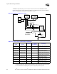
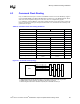
Only one differential clock pair is routed to each DIMM connector because the MCH only supports
registered DDR DIMMs. All CMDCLK/CMDCLK# termination is on the DIMM modules. Route
each clock and its compliment adjacent to each other. The two complimentary signals
(e.g., CMDCLK_x0 and CMDCLK_x0#) must be length matched to each other within ± 2 mils and
must be routed on the same layer. If a layer transition must occur, minimize the discontinuity in the
ground reference plane.
NOTES:
1. CMDCLK/CMDCLK# must be matched to within ± 2 mils using package trace length compensation.
2. 3-DIMM solution: Treat the CMDCLK_x3/CMDCLK_x3# pair as a no connect.
3. Indicated lengths measured from the MCH component pin to the DIMM connector pin.
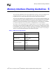
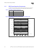
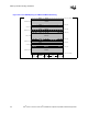
Table 6-5. Command Clock Pair Routing Guidelines
Parameter 3-DIMM Solution 4-DIMM Solution Reference
Signal Group CMDCLK, CMDCLK#
Topology Point-to-point Figure 6-7
Reference Plane Ground Figure 6-8
Differential Trace Impedance (Z
0
) 100 Ω ± 10% 100 Ω ± 10% Figure 6-8
Nominal Trace Width 5 mil 5 mil Figure 6-8
Differential Trace Spacing 7.5 mil 7.5 mil Figure 6-8
Group Trace Spacing 20 mil 20 mil Figure 6-8
MCH to DIMM1 Trace Length 4.0" ± 250 mil 7.50" ± 100 mil Figure 6-7
MCH to DIMM2 Trace Length 6.0" ± 250 mil 8.00" ± 100 mil Figure 6-7
MCH to DIMM3 Trace Length 8.0” ± 250 mil 8.75" ± 100 mil Figure 6-7
MCH to DIMM4 Trace Length Not Supported 10.75" ± 100 mil Figure 6-7
MCH Breakout Guidelines 5/5, < 500 mil 5/5, < 500 mil
Length Tuning Requirements
CMDCLK to CMDCLK#:
±2 mil
CMDCLK to CMDCLK#:
±2 mil
Figure 6-7
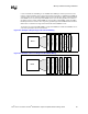
Figure 6-7. Command Clock Topology
DIMMs
CMDCLK_x0 and CMDCLK_x0#
MCH
CMDCLK_x1 and CMDCLK_x1#
CMDCLK_x2 and CMDCLK_x2#
CMDCLK_x3 and CMDCLK_x3#