
Intel Xeon Processor and Intel E7500/E7501Chipset Compatible Platform Design Guide


Platform Power Delivery Guidelines
178 Intel
®
Xeon™ Processor and Intel
®
E7500/E7501 Chipset Compatible Platform Design Guide
The data bus must route over a uniform power plane because of signal quality constraints.
Consequently, in a multiprocessor system design, a single power plane should be used for power
delivery to all processors. Multiple processors operating at different voltages are not supported, and
will not be validated by Intel.
The processor VCCSENSE and VSSSENSE pins must be routed to vias. The vias should be as
close to the socket pins as possible and should be connected with low impedance traces. Because
these signals provide measurement points to verify adherence to the processor's VCC_CPU
specifications, the vias need to be accessible to measurement equipment. These pins must not be
used as SENSE lines to the VRs.
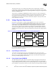
11.2.3 Voltage Regulator Requirements
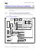
Intel requires a local VRM 9.1-compliant Voltage Regulator for VCC_CPU. As shown in
Figure 11-3, it can be either one Voltage Regulator Module (VRM 9.1) DC-to-DC converter for
each processor, or one Voltage Regulator-Down (VRD) solution for both processors in a DP
system. Refer to either VRM 9.1 DC-DC Converter Design Guidelines or Dual Intel
®
Xeon™
Processor Voltage Regulator Down (VRD) Design Guidelines for Voltage Regulator tolerance
specifications (regulation requirements at the voltage regulator remote sense point located at the
geometric center of the processors). These two documents are referred to as the voltage regulator
guidelines.
The voltage regulator should be capable of accepting a 5-bit VID code, which is used to indicate
the maximum voltage allowed by the individual processor unit. The VID values are documented in
the Intel
®
Xeon™ Processor Datasheet.
11.2.3.1 Input Voltages and Currents
To minimize power distribution losses, the recommended main power source for the VR is
12 V +5%,
– 8%. This voltage is supplied by a conventional server power supply such as the SSI
EPS-12 V. The system designer should ensure that the input circuit of the VR incorporates the
necessary local bulk bypassing on the 12 V rail.
11.2.3.2 Power Good Output (PWRGD)
The VR should provide an open collector or equivalent Power Good signal consistent with TTL
DC levels. This signal should transition to the open (>100 k
Ω) state within 10 ms of the output
voltage stabilizing within the specified processor operating voltage range. The signal should be in
the low impedance (to ground) state when VCC_CPU is outside of the required range, and should
Figure 11-3. Power Distribution Block Diagrams for DP System Motherboard
Power
Supply
Voltage Regulator Module 1
Voltage Regulator Module 2
Processor 0
Processor 1
Power
Supply
Voltage Regulator
Down
Processor 0
Processor 1