
Intel Xeon Processor Multiprocessor Platform Design Guide


25
Clock Routing Guidelines
Clock Routing Guidelines 5
5.1 System Bus Clocking Guidelines
5.1.1 Routing Guidelines for BCLK[1:0]
Note: For designs using non-Intel chipsets please contact the corresponding chipset vendor for specific
information regarding clock driver and baseboard design requirements.
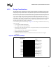
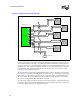
To minimize jitter and improve routing, the 4-way Intel Xeon processor MP and Intel Xeon
processor MP with up to 2-MB L3 cache on the 0.13 micron process system may use a dual-chip
clock solution. The first component (referred to as CKx_WBY) is shown in Figure 5-1. In this
configuration the main clock generator provides six, 100 MHz differential outputs for all of the
system bus agents, one 14.31 MHz output, and one, 66 MHz speed clock that drives a second
system clock chip referred to as CKFF, which provides additional system clocks such as PCI.
Figure 5-1 shows the implementation of the system bus clocks for this configuration. Refer to the
CK00 Clock Synthesizer/Driver Design Guidelines for complete information about CKx_WBY
and CKFF.
When connecting CK00 HOST clock and HOST_BAR clock to host agent BCLK0 and BCLK1 be
consistent across all host agents. In other words, connect HOST pin to BCLK0 and HOST_BAR
pin to BCLK1 for each system bus agent.