
Intel Xeon Processor and Intel E7500/E7501Chipset Compatible Platform Design Guide


Intel
®
Xeon™ Processor and Intel
®
E7500/E7501 Chipset Compatible Platform Design Guide 251
Layout Checklist
14.3 MCH Layout Checklist
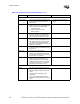
Table 14-3. MCH Layout Checklist (Sheet 1 of 3)
Checklist Items Recommendations Comments
Host Interface
ADS#
AP[1:0]
BINIT#
BNR#
BPRI#
BREQ0#
1
CPURST#
2
DBSY#
DEFER#
HA[35:3]#
3
HD[63:0]#
4
HADSTB[1:0]#
5
HDSTBN[3:0]#
6
HDSTBP[3:0]#
7
HIT#
HITM#
HLOCK#
HREQ[4:0]#
8
HTRDY#
9
DP[3:0]#
DRDY#
RS[2:0]#
RSP#
XERR#
10
DBI[3:0]#
• See processor section of this checklist.
DDR Interfaces A & B / Connector
General
Guidelines
• 5 on 15 is maintained for Data/Strobe/
CMD signals; 5 on 7.5 is maintained for
CMDCLK_x/CMDCLK_x# signals.
• If using the recommended stack-up, outer
layer routing of DDR signals should be
kept to a minimum (except for reference
voltages). Via up close to passive
devices, and immediately via back down
following the device.
• Try to maintain same ground reference
when transitioning layers—add stitching
via if reference plane changes.
• Connect termination resistors directly to
termination plane (flood is on outer layer).
• Space traces out as much as possible
through the DIMMs.
DQ_x[63:0]
CB_x[7:0]
DQS_x[17:0]
• Route entirely on the same layer from
MCH to DIMM to termination (no layer
transitions). Place the series resistor <
800 mils from the first DIMM connector.
All signals in a data group must be length
matched to the associated DQS within
± 25 mils. Place termination resistor
within 800 mils from the last DIMM
connector.
• Refer to Section 6.2.