
Intel Xeon Processor and Intel E7500/E7501Chipset Compatible Platform Design Guide

Intel
®
Xeon™ Processor and Intel
®
E7500/E7501 Chipset Compatible Platform Design Guide 219
High-Speed Design Concerns
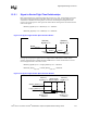
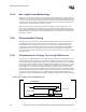
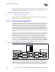
To compensate for package-induced skew, all source synchronous motherboard trace lengths are
adjusted by the exact amount of Package Length Compensation (PLC). Equation 12-3 defines PLC
for a particular signal. Signal X is any signal in the group that does not have the longest package
length. This includes the strobe signals.
Equation 12-3. Package Length Compensation (PLC) Definition
SignalX
PLC
= Maximum_Signal_in_Group
Package Length
- SignalX
Package Length
The signals with a package length less than the longest package trace in that group will require
additional motherboard trace length equal to SignalX
PLC
. Equation 12-3 yields a zero PLC for the
signal with the longest package length. So the signal with the longest package length would require
no amount of additional motherboard trace length. Figure 12-14 illustrates PLC using a data signal
as the longest package trace and strobe signal as “Signal X”.
12.6.2 Signal Integrity Adjustment Factor
The second factor in length matching the system bus source synchronous signals involves adjusting
motherboard trace lengths to compensate for signal integrity effects that will affect the relationship
of the signal and associated strobe at each receiver. The signal integrity effects include edge rate
degradation and reflections caused by the stubs created by the Processor 1 package. These stub
lengths act as capacitive loads and transmission lines, and thus degrade the edge rate as the signal
travels from Processor 0 to the MCH and from the MCH to Processor 0.
The Processor 0 signals with longer stubs will see more degradation than those with shorter stubs.
For source synchronous signals, the goal is to reduce skew between a signal and its associated
strobe. Since strobe signals typically have short package lengths, they will not see much edge rate
degradation. However, since other signals can have stub lengths up to approximately 600 mils, the
edge rate degradation can be dramatic relative to that of the strobe. These large differences in the
slope and shape of the edges at the receiver results in a significant skew between the longer and
shorter signals within the same signal group. I.e. the additional noise of longer processor package
signals will cause them to cross the VREF threshold at a later time than the shorter processor
package signals. The net effect could result in source synchronous timing violations if
uncompensated.
To compensate for this signal integrity degradation, a specific length is added to the motherboard
trace lengths for signals that have shorter stub lengths. This will achieve similar VREF threshold
crossing times for a signal and its strobe at the receiver. This motherboard length is referred to as
the Signal Integrity (SI) Adjustment Length. The methodology for calculating SI Adjustment
Length is dependent on the system bus topology, edge rates of the processor and MCH, signal
velocities for package and motherboard, VCC_CPU termination voltage, I/O capacitance of the
Figure 12-14. Example of PLC Compensation on the Motherboard
Longest Package T race
Shortest Package T race
Die Pad
Die Pad
Component Pin
PLC
Shortest Motherboard Trace
Component A
Routes to
Component B
Strobe Signal
Data Signal
Shortest Motherboard Trace
Delta
Delta