
Dual Intel Xeon Processor Voltage Regulator Down (VRD) Design Guidelines


Dual Intel
®
Xeon™ Processor Voltage Regulator Down (VRD) Guidelines
21
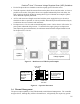
Each of the phase drivers should be somewhat equally spaced from the socket.
The bulk capacitors should be mounted between the phase drivers and the socket, as close as
possible to the socket. If the phase drivers are separated substantially from each other, the
bulk capacitors should be divided up among them. Figure 14 details one example of phase
driver and bulk capacitor placement.
All Vcc and return trace lengths associated with the power supply delivery to the socket
should be as short as possible, as wide as possible, and multi-layered with interleaved layers,
to minimize the trace resistance and inductance.
Each processor’s 603 vias (and associated antipads) create a “Swiss cheese” effect in the V
CC
power plane underneath the processor. To maximize the copper going to each processor
(thus improving power distribution), the minimum manufacturable antipad should be used
for the processor’s 603 vias.
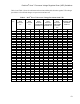
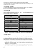
Voltage
regulator
Voltage regulator
Voltage
regulator
Voltage regulator
Figure 13 – Dual-Processor VRD Layout Examples
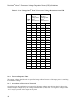
Address and
Cntrl Pins
Data Pins
4-6 0.1[uF] with
603 body over the
data signals and as
close to the CPU
package as
possible
4-6 0.1[uF] with
603 body over the
data signals and as
close to the
package as
possible
3-4 0.1[uF] with 603
body over the address
and cntrl signals and
as close to the chipset
package as possible
3-4 0.1[uF] with 603
body over the address
and cntrl signals and
as close to the
package as possible
Cavity under
Processor
Figure 14 – Capacitor Placement
3.4 Thermal Management
The power output capability of the VRD demands careful thermal management. The controller
and gate drivers, although they will have thermal losses, will generally not require any special