
Intel Xeon Processor and Intel E7500/E7501Chipset Compatible Platform Design Guide

Schematic Checklist
232 Intel
®
Xeon™ Processor and Intel
®
E7500/E7501 Chipset Compatible Platform Design Guide
13.3 Intel
®
ICH3-S Schematic Checklist
Note: There are no inputs to the ICH3-S that can be left floating.
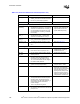
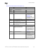
Table 13-3. Intel
®
ICH3-S Schematic Checklist (Sheet 1 of 6)
Checklist Items Recommendations Comments
Processor Signals
A20M#
CPUPWRGD
CPUSLP#
(SLP#)
FERR#
IGNNE#
INIT#
LINT1
1
LINT0
1
SMI#
STPCLK#
• Refer to the signal recommendations under
the Processor Schematic Checklist.
RCIN#
A20GATE
• Pull-up is required if driven by an open drain
signal (the value of the resistor is
determined by the driver), otherwise none
needed.
• Typically driven by Open Drain
external Micro-controller.
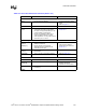
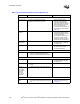
FWH Interface
FWH[3:0]/ LAD[3:0]
LDRQ[1:0]
• No extra pull-ups required. Connect straight
to FWH/LPC and, if supported, a BMC.
• Intel
®
ICH3-S Integrates 24 kΩ
pull-up resistors on these signal
lines.
GPIO
GPIO[7:0] • Unused core well inputs must use a
8.2 k
Ω – 10 kΩ pull-up to 3.3 V.
• GPIO[1:0] can be used as REQ[B:A]#.
• GPIO[1] can be used as PCI REQ[5]#.
• GPIO[5:2] can be used as PIRQ[H:E]#.
• These signals are 5 V tolerant.
• These pins are in the Main
Power Well. Pull-ups must use
the 3.3 V plane.
• Ensure all unconnected signals
are
outputs only.
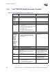
GPIO[8] and
GPIO[13:11]
• Unused resume well inputs must use a
8.2 k
Ω – 10 kΩ pull-up to VCCSUS3_3.
• These are the only GPIs that can be used
as ACPI compliant wake events.
• These signals are not 5 V tolerant.
• GPIO[11] can be used as SMBALERT#.
• These pins are in the resume
power well. Pull-ups go to
VCCSUS3_3 plane.
• These are the only GPI signals
in the resume well with
associated status bits in the
GPE1_STS register.
GPIO[23:16] • GPIO[22] is open drain.
• GPIO[17:16] can be used as GNT[B:A]#.
• GPIO[17] can be used as PCI GNT[5]#.
• Fixed as output only. Can be
left NC.
• In main power well.
GPIO[28,27,25,24] • Can be left NC.
• From resume power well (VCCSUS3_3).
• I/O pins. Defaults as an output.
GPIO[43:32] • From main power well (3.3 V). • I/O pins. Defaults as an output
when enabled as GPIOs.