
Intel Xeon Processor and Intel E7500/E7501Chipset Compatible Platform Design Guide

Intel
®
Xeon™ Processor and Intel
®
E7500/E7501 Chipset Compatible Platform Design Guide 205
High-Speed Design Concerns
High-Speed Design Concerns 12
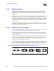
12.1 Return Path
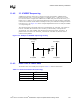
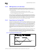
The return path is the route current takes to return to its source. It may take a path through ground
planes, power planes, other signals, or integrated circuits. The return path is based on electro-
magnetic field effects. It is useful to think of the return path as the path of least impedance nearest
the signal conductor. Discontinuities in the return path often have signal integrity and timing
effects that are similar to the discontinuities in the signal conductor. Therefore, the return paths
must be given similar considerations. A simple way to evaluate return path parasitic inductance is
to draw a loop that traces the current from the driver through the signal conductor to the receiver,
and then back through the ground/power plane to the driver again. The smaller the area of the loop,
the lower the parasitic inductance.
The following sets of return path rules apply to all designs:
• Always trace out the return current path and provide as much care to the return path as the path
of the signal conductor.
• Do not allow splits in the reference planes in the path of the return current.
• Do not allow routing of signals on the reference planes near system bus signals.
• Do not allow signal layer changes that force the return path to make a reference plane change,
even if it is from one ground layer to another ground layer.
• Decoupling capacitors do not adequately compensate for a plane split.
• Do not route over via anti-pads or socket anti-pads
If reference plane changes must be made:
• Change from a ground reference to a ground reference and place a via that connects the two
planes as close as possible to the signal via. This also applies when making a change from
VCC to VCC.
• For symmetric stripline, return path vias for both ground and VCC must be provided.
• Do not switch reference from VCC to ground or vice versa.
12.2 Decoupling Theory
The primary objective of the decoupling guidelines is to minimize the impact of return path
discontinuities and to ensure that the I/O has adequate power decoupling. The worst-case return
path discontinuity anticipated is for systems that use microstrip structures on the motherboard. If a
motherboard uses symmetric stripline with VCC and ground references, then a discontinuity does
not exist and additional decoupling is not necessary. If the motherboard routing references only a
single reference plane (VCC or ground), then a return path discontinuity exists.
The inductance of the system due to cables and power planes slows the power supply's ability to
respond quickly to a current transient. Decoupling a power plane can be broken into several
independent parts. The closer to the load the capacitor is placed, the more inductance is bypassed.
By bypassing the inductance of leads, power planes etc., less capacitance is required. However,
closer to the load there is less room for capacitance. Therefore, trade-offs must be made.