
Intel Xeon Processor and Intel E7500/E7501Chipset Compatible Platform Design Guide

Intel
®
Xeon™ Processor and Intel
®
E7500/E7501 Chipset Compatible Platform Design Guide 197
Platform Power Delivery Guidelines
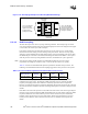
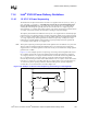
When designing the VCCA1_2 filter (Figure 11-20), follow these guidelines:
• One 54 nH Inductor close to the edge of the package (within 1 inch of the die).
• One 100 µF or 150 µF LF capacitor close to the edge of the package.
• Minimum of two (four preferred) Low ESL HF capacitors, 0.22 µF or 0.1 µF, on the backside
of the motherboard under the die.
• Route the VCCA1_2 trace 1 inch, 35 mils wide with 15-mils spacing on three signal layers of
the motherboard; connect to VCCA1_2 island on signal layers directly under the MCH core.
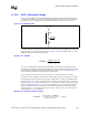
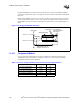
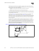
When designing the VCCA1_2 and VCCACPU filters (Figure 11-21 and Figure 11-22), follow
these guidelines:
• One 100 nH Inductor close to the edge of the package (within 1 inch of the die).
• One 100 µF or 150 µF LF capacitor close to the edge of the package.
• Minimum of one Low ESL HF capacitor, 0.1 µF on the motherboard backside, under the die.
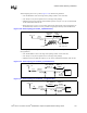
Figure 11-20. Filter Topology for VCCA1_2 (DDR Interface)
VCC_1.2
VCCA_1.2
54 nH
MCH
Within 1"
of Ball
RC Network
Within 1"
100 µF
Route to Balls P20,
T20, V20, Y20,
Y18, Y16, Y14
0.1 µF
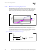
Figure 11-21. Filter Topology for VCCAHI1_2 (HUB Interface)
Figure 11-22. Filter Topology for VCCACPU_1.2 (System Bus)
VCC_1.2
100 nH
1 Ω
VCCAHI_1.2
100 µF
0.1 µF
MCH
RLC Network
Within 1"
Within 1"
of Ball
Route to
ball P16
VCC_1.2
100 nH
1 Ω
VCCACPU1_2
100 µF
0.1 µF
MCH
RLC Network
Within 1"
Within 1"
of Ball
Route to
ball U15