
Intel Xeon Processor Multiprocessor Platform Design Guide

92
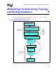
Methodology for Determining Topology and Routing Guidelines
The design process should begin with an initial timing analysis and topology definition. Pre-layout
analog simulations should be performed. These pre-layout simulations will help define routing
rules prior to placement and routing. After routing, the interconnect database can be extracted and
post-layout simulations can be performed to refine the timing and signal integrity analysis. The
analog simulations should be validated when actual systems become available. Target
measurements of the high-significance parameters to ensure they fall within simulated boundaries.
Pre-layout simulations provide a detailed picture of the working solution space that meets flight
time and signal quality requirements. By basing board layout guidelines on the solution space, the
iterations between layout and post-layout simulation can be reduced.
Intel recommends running simulations at the device pads for signal quality and for timing analysis.
However, simulation results at the device pins may be used later to correlate simulation
performance against actual system measurements.
Pre-layout analysis includes a sensitivity analysis using parametric sweeps. Parametric sweep
analysis involves varying one or two system parameters while all others such as driver strength,
package Z
0
, and S
0
are held constant. This way, the sensitivity of the proposed bus topology to
varying parameters can be analyzed systematically. Sensitivity of the bus to flight times and signal
quality should be covered. Suggested sweep parameters include trace lengths, termination resistor
values, and any other factors that may affect flight time, signal quality, and feasibility of layout.
Minimum flight time and worst signal quality are typically analyzed using fast I/O buffers and
interconnect. Maximum flight time is typically analyzed using slow I/O buffers and slow
interconnects. However, fast I/O buffers and various baseboard and package combinations have
been found to have violating signal quality. It is advisable to perform some level of Monte Carlo
analysis, which includes all possible parameters.
Outputs from each sweep should be analyzed to determine which regions meet timing and signal
quality specifications. To establish the working solution space, find the common space across all
the sweeps that result in passing timing and signal quality. The solution space should allow enough
design flexibility for a feasible, cost-effective layout.
The effects of ISI and return path irregularities are difficult and tedious to simulate with 100%
accuracy. Intel has found through experimentation and targeted simulations that these effects can
have a significant impact on the primary signal. Due to the findings of this work, Intel has been
able to more accurately predict the effects. Given the complexity of a quad-pumped source
synchronous bus architecture, it was necessary for Intel to tighten the component timings and bus
requirements in order to provide a viable routing solution space. Because of this, Intel strongly
recommends adhering to the design guideline requirements and component specifications.
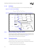
9.1 Timing Methodology
The timing equations used for both source synchronous and common clock parameters are derived
in the following sections.
9.1.1 Source Synchronous
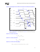
In a source synchronous bus the clock (or strobe) is driven from the same source as the signal it
will sample. The strobe and the signal both propagate to the receiver via the PCB. The receiver
then uses the strobe to sample the signal. This eliminates the need to account for worst-case flight
times and, in theory, will significantly increase the maximum bus speed.