
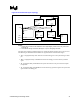
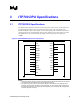
ITP700 Debug Port Design Guide


R
40 ITP700 Debug Port Design Guide
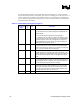
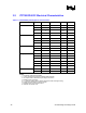
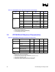
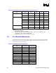
Table 22. ITP700 DPA Execution Signal AC Electrical Characteristics
Signal Parameter Min Max Unit Note
Setup 400 ps 1 BPM[5:0]#, RESET
Hold 200 ps 1
Rise Time 5 ns 2
Fall Time 5 ns 2
Period 5 15 ns 3
Time High 2.2 ns
BCLK(p/n)
Time Low 2.2 ns
Rise Time 1 4 ns 2, 4 BPM5DR#
Fall Time 8 15 ns 2, 4
NOTES:
1. With respect to BCLK(p/n).
2. Measured from 20% to 80% of transition.
3. Specification for valid synchronous operation of the ITP. Asynchronous operation has no Max
specification but shares the Min specification listed.
4. Measured into a load to 1.5 V of 50 Ω s and 35 pF to GND.
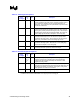
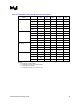
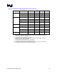
3.4 Pin Absolute Maximums
The following data represents the maximum voltage that the pins of the ITP can sustain without
damage. These values do not reflect a valid operating range. See DC specification sections for
valid operating ranges for each signal.
Table 23. P700 DPA Pin Absolute Maximums
Signal Voltage Low Voltage High
PWR 0 V 5 V
BCLK -1.2 V 2.5 V
DBA# DBR# -0.5 V 5 V
FBI -0.5 V 4.6 V
FBO -1.2 V 2.5 V
TCK -0.5 V 4.6 V
TMS -0.5 V 4.6 V
TDI -0.5 V 4.6 V
TDO -1.2 V 2.5 V
TRST# -0.5 V 4.6 V
BPM[5:0]#, -1.2 V 3.3 V
BPM5DR# -0.5 V 5 V
RESET# -1.2 V 3.3 V