
Intel Xeon Processor and Intel E7500/E7501Chipset Compatible Platform Design Guide

Schematic Checklist
226 Intel
®
Xeon™ Processor and Intel
®
E7500/E7501 Chipset Compatible Platform Design Guide
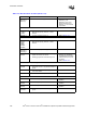
BPM[5:0]# • For all ITP interface signal
schematic, layout and routing
recommendations, refer to the
ITP700 Debug Port Design Guide.
BR[3:0]# • Connect BR[0]# to the MCH’s BREQ0# pin,
Processor 0’s BR0# pin, and Processor 1’s
BR1# pin. Terminate using a 50
Ω ± 5% pull-
up resistor at Processor 0.
• Connect BR[1]# signal to Processor 0’s
BR1# pin and Processor 1’s BR0# pin.
Terminate both ends of the bus using
50
Ω ± 5% pull-up resistors.
• BR[3:2]# should be pulled-up to VCC_CPU
using a 50
Ω ± 5% individually at each
processor or be connected between
processors and terminated at one end.
• BR0# is an AGTL+ Common
Clock I/O.
• BR[3:1]# are AGTL+ Common
Clock Inputs.
• These signals do not have on-die
processor termination and must
be terminated on the
motherboard.
• Refer to Section 5.2.3.
BSEL[1:0] • Connect to external comparator logic that
verifies both processors are specified to
operate at the same system bus frequency.
Also use these signals to select the clock
driver to operate at either 100 or 133 MHz.
•1 k
Ω 5% pull-up to 3.3 V, if using
recommended circuit.
• Driven by processor to indicate
specified system bus frequency.
• Refer to Section 5.6.3.
COMP[1:0] • Terminate to ground separately using
49.9
Ω ± 1% resistors.
• Power/Other.
• Refer to Section 5.3.3.
GTLREF[3:0] • 49.9
Ω ± 1% pull-up to VCC_CPU.
• 84.5
Ω ± 1% pulldown to ground.
• At the divider, decouple with a 1 µF and at
the component pin, decouple with a 220 pF.
• Power/Other.
• Refer to Section 11.2.10.
ODTEN • Enable on-die termination (ODT) on
Processor 0 (end processor) by pulling up to
VCC_CPU with a 50
Ω ± 20% resistor.
• Disable ODT for Processor 1 by pulling down
to ground with a 50
Ω ± 20% resistor.
• Input.
• Refer to Section 5.3.4.
PWRGOOD
(CPUPWRGOOD)
• 300
Ω ± 5% pull-up to VCC_CPU.
• Connect to both processors and ICH3-S.
• Power/Other.
• Refer to Section 5.3.1.
Reserved • Reserved signals must remain as No
Connect (NC).
RESET#
7
• 51 Ω ± 5% pull-up to VCC_CPU.
• Connect to MCH and both processors. Note
that this signal is dual terminated at both
ends of transmission line.
• AGTL+ Common Clock Input.
• Refer to Section 5.2.2.
• If using ITP, for signal connection
to ITP, refer to the
ITP700 Debug
Port Design Guide
for all
schematic, layout and routing
recommendations.
SKTOCC# • If supported, pull-up to 3.3 V and use in
external logic to detect whether one or two
processors are installed.
• If unused, leave as NC.
• Power/Other
• Refer to Section 5.6.2.
Table 13-1. Processor Schematic Checklist (Sheet 2 of 4)
Checklist Items Recommendations Comments