
Technical Product Specification


Appendix A: Integration and Usage Tips Intel® Server Board S2600IP and Intel® Workstation Board W2600CR TPS
118 Intel order number G34153-004 Revision 1.4
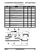
Output
Step Load Size
(See note 2)
Load Slew Rate
Test Capacitive Load
12V1+12V2+12V3
23A
0.5 A/sec
2200 F
1,2
+5VSB
0.5A
0.5 A/sec
20 F
Notes:
1. Step loads on each 12V output may happen simultaneously.
2. The +12V should be tested with 2200F evenly split between the four +12V rails.
3. This will be tested over the range of load conditions in section 9.4.2.
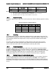
9.4.6 Capacitive Loading
The power supply shall be stable and meet all requirements with the following capacitive loading
ranges.
Table 68. Capacitive Loading Conditions
Output
Min
Max
Units
+3.3V
250
5000
F
+5V
400
5000
F
+12V
500
8000
F
-12V
1
350
F
+5VSB
20
350
F
9.4.7 Grounding
The output ground of the pins of the power supply provides the output power return path. The
output connector ground pins shall be connected to the safety ground (power supply enclosure).
This grounding should be well designed to ensure passing the max allowed Common Mode
Noise levels.
The power supply shall be provided with a reliable protective earth ground. All secondary
circuits shall be connected to protective earth ground. Resistance of the ground returns to
chassis shall not exceed 1.0 m. This path may be used to carry DC current.
9.4.8 Closed loop stability
The power supply shall be unconditionally stable under all line/load/transient load conditions
including capacitive load ranges specified in Section 4.6. A minimum of 45 degrees phase
margin and -10dB-gain margin is required. The power supply manufacturer shall provide proof
of the unit’s closed-loop stability with local sensing through the submission of Bode plots.
Closed-loop stability must be ensured at the maximum and minimum loads as applicable.
9.4.9 Residual Voltage Immunity in Standby mode
The power supply should be immune to any residual voltage placed on its outputs (Typically a
leakage voltage through the system from standby output) up to 500mV. There shall be no
additional heat generated, nor stressing of any internal components with this voltage applied to
any individual or all outputs simultaneously. It also should not trip the protection circuits during
turn on.