
Universal Peripheral Interface User's Manual

UPI-C42/UPI-L42
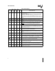
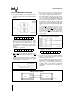
Table 1. Pin Description (Continued)
DIP PLCC QFP
Symbol Pin Pin Pin Type Name and Function
No. No. No.
P
20
–P
27
21–24 24–27 39–42 I/O PORT 2: 8-bit, PORT 2 quasi-bidirectional I/O lines. The lower 4 bits
(P
20
–P
23
) interface directly to the 8243 I/O expander device and
35–38 39–42 11, 13–15
contain address and data information during PORT 4– 7 access. P
21
can be programmed to provide hardware A20 gate support. The upper
4 bits (P
24
–P
27
) can be programmed to provide interrupt Request and
DMA Handshake capability. Software control can configure P
24
as
Output Buffer Full (OBF) interrupt, P
25
as Input Buffer Full (IBF)
interrupt, P
26
as DMA Request (DRQ), and P
27
as DMA ACKnowledge
(DACK
).
PROG 25 28 43 I/O PROGRAM: Multifunction pin used as the program pulse input during
PROM programming.
During I/O expander access the PROG pin acts as an address/data
strobe to the 8243. This pin should be tied high if unused.
V
CC
40 44 17 POWER:
a
5V main power supply pin.
V
DD
26 29 1 POWER:
a
5V during normal operation.
a
12.75V during programming
operation. Low power standby supply pin.
V
SS
20 22 38 GROUND: Circuit ground potential.
290414–4
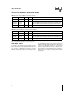
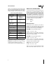
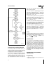
Figure 4. Block Diagram
3