TE430VX Motherboard Technical Product Specification Order Number 281817-003 May 1996
Revision History Revision Revision History Date -003 Fixed drawing designators, added USB module, corrected inaccuracies, reworded sections for clarity, removed reference to Creative Labs Vibra 16S with Yamaha FM Synthesis 5/96 -002 Changed Name of product from Advanced/TE to TE430VX throughout 4/96 -001 Preliminary release of the TE430VX Technical Product Specification. 3/96 This product specification applies only to standard TE430VX ATX motherboards with BIOS identifier 1.00.01.CY0.
Table of Contents 1 Motherboard Description 1.1 1.2 1.3 1.4 Overview ............................................................................................................7 Motherboard Manufacturing Options..................................................................9 Form Factor .......................................................................................................9 Microprocessor.................................................................................................
TE430VX Motherboard Technical Product Specification 1.11 1.12 1.13 1.14 1.15 1.10.4 Power Connector - J7M2 ....................................................................18 1.10.5 Floppy Drive Connector - J10H1 ........................................................19 1.10.6 IDE Connectors - J9H1, J9H2.............................................................19 1.10.7 Front Panel I/O Connectors - J9E2.....................................................20 1.10.
Contents 3 Motherboard BIOS and Setup Utility 3.1 3.2 3.3 3.4 3.5 3.6 3.7 3.8 3.9 3.10 3.11 3.12 Introduction ......................................................................................................41 BIOS Flash Memory Organization ...................................................................41 BIOS Upgrades ................................................................................................42 PCI IDE Support..................................................................
1 Motherboard Description 1.1 Overview The TE430VX design accepts Pentium processors operating at 75 MHz, 90 MHz, 100 MHz, 120 MHz, 133 MHz, 150 MHz, 166 MHz, and 200MHz. There is an option of having 256 KB of Pipeline Burst SRAM soldered onto the motherboard, or a Card Edge Low Profile (CELP) connector for cache expandability. The memory subsystem is designed to support up to 128 MB of EDO DRAM, or up to 64 MB of a new memory architecture called SDRAM, in standard 168-pin DIMM sockets.
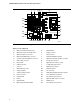
TE430VX Motherboard Technical Product Specification A B G CDE F P H HH I GG Q FF J K L M EE R DD N CC O BB AA Z Y X W V U T S OM04814 Figure 1. Motherboard Features Tigereye board diagram 8 A. Optional Yamaha† FM synthesizer R. 82430VX TDX B. Optional Creative Labs Audio device S. Floppy connector C. Optional telephony connector T IDE connectors D. Optional CD-ROM audio connector U. PIIX3 PCI/ISA/IDE Xcelerator E. Creative Labs ModemBlaster connector V.
Motherboard Description 1.2 Motherboard Manufacturing Options • • • • • • Creative Labs Vibra 16C Audio S3 Trio64V+ Video CELP Module or soldered 256k PBSRAM with GWE USB Split Plane Voltage Support for Socket 7 Flash Recovery 1.3 Form Factor The motherboard is designed to fit standard ATX form factor chassis. Figure 2 illustrates the motherboard’s dimensions. The motherboard meets the standard ATX specification guidelines in that the outer dimensions are 12" x 9.6".
TE430VX Motherboard Technical Product Specification 1.4 Microprocessor The motherboard is designed to operate with 3.3 volt Pentium Processors running at 75, 90, 100, 120, 133, 150, 166, and 200MHz. An onboard linear voltage regulator circuit provides the required 3.3 volts from the 5.0 volt tap of the power supply. An on-board jumper enables use of VRE specified processors. The Pentium processor maintains full backward compatibility with 8086, 80286, i386 and Intel486 processors.
Motherboard Description 1.5.1.2 SDRAM Synchronous Dynamic Random Access Memory, (SDRAM) is designed to improve main memory performance. SDRAM is synchronous to the memory clock unlike standard Fast Page DRAM, or EDO DRAM. All the timing is dependent on the number of memory clock cycles. This makes the timing design simpler and makes a faster memory speed easier to achieve. Discrete SDRAM components must meet the 66 MHz PC SDRAM Specification version 1.0 to function correctly. 1.5.
1.6.2 82430VX Data Path (TDX) Two 82430VX TDX data path components provide a 64-bit microprocessor to memory path. The TDX components are controlled by the TVX. They each add one load to the PCI bus and perform all of the required byte and word swapping. The TDX devices come in a 208 pin QFP package. 1.6.3 PCI ISA/IDE Xcelerator (PIIX3) The PIIX3 provides the interface between the PCI and ISA buses and integrates a dual channel fast IDE interface capable of supporting up to 4 devices.
Motherboard Description 1.7 Ultra I/O Interface Controller (SMC FDC37C93FR) 1.7.1 Floppy controller The SMC FDC37C93FR is software compatible with the DP8473 and 82077 floppy disk controllers. The floppy interface can be configured for 360 KB or 1.2 MB 5¼" media or for 720 KB, 1.2 MB, 1.44 MB, or 2.88 MB 3½" media in the BIOS setup. By default, the Floppy A interface is configured for 1.44 MB and Floppy B is disabled. Another setup option prevents the user from being able to write to floppy.
TE430VX Motherboard Technical Product Specification 1.7.4 IrDA (infra-red) support A 5-pin interface on the front panel I/O connector is provided to allow connection to a Hewlett Packard† HSDSL-1000 compatible Infra-red (IrDA) transmitter/receiver. Once the module is connected to the front panel I/O header, Serial port 2 can be re-directed to the IrDA module.
Motherboard Description 1.8.1 Resolutions supported Table 1. Graphics Resolutions Supported by Supported by Resolution 1 MB DRAM 2 MB DRAM 640x480x16 colors Yes Yes 640x480x256 colors Yes Yes 60,72,75,85 640x480x64k colors Yes Yes 60,72,75 640x480x16.7m colors No Yes 60,72,75 800x600x256 colors Yes Yes 56,60,72,75,85 800x600x64k colors Yes Yes 60,72,75 800x600x16.
TE430VX Motherboard Technical Product Specification The audio subsystem requires up to two DMA channels (to support full duplex operation) and one interrupt. When the Vibra 16C is programmed for full duplex operation, two DMA channels are assigned: one of the channels will be a 16-bit channel and the other will be 8 bits. The system can be configured to use either DMA channels 1 or 3 (8 bit channels) and DMA channels 5 or 7 (16 bit channels). The interrupt can be mapped to IRQ 5, 7, 9, or 10.
Motherboard Description 1.10 Motherboard Connectors Figure 3 shows the connectors on the motherboard. Pin call outs and signal names follow Figure 3. J1F1 2 1 10 9 Mod-blast Connector J2F3 J2F2 J2F1 1 2 1 4 CDROM Connector Telephony Connector 7 Wave Table Connector 1 DIMM Sockets(2) A(J3F1) B(J3G1) CELP Cache Socket PCI Connectors(4) (J2J1) J2C1, J2D1 J2E1, J2E2 J7L1 6 AB ISA Connectors(3) J1A1, J1A2 J1B1 2 20 J7M2 40 J9H1 J9H2 1 2 J9E2 27 1 20 39 PCI IDE Connector(2) 1 3.
TE430VX Motherboard Technical Product Specification 1.10.1 Pin Signal Name 1 Ground 2 CD Audio Left Speaker 3 Ground 4 CD Audio Right Speaker 1.10.2 Wave Table Connector - J2F3 Pin Signal Name 1 Wave Right 2 Ground 3 Wave Left 4 Ground 5 Key 6 Ground 7 MIDI_In 8 MIDI Out 1.10.3 Telephony Connector - J2F1 Pin Signal Name 1 Mic In 2 Ground 3 Mono Out 4 Key 1.10.4 18 CD-ROM Connector - J2F2 Power Connector - J7M2 Pin Signal Name Pin Signal Name 1 +3.
Motherboard Description 1.10.
TE430VX Motherboard Technical Product Specification IDE Connectors - J9H1, J9H2 (continued) Pin Signal Name Pin Signal Name 29 DDACK0 (DDACK1) # 30 Ground 31 IRQ14 (IRQ15) 32 Reserved 33 Addr 1 34 Reserved 35 Addr 0 36 Addr 2 37 Chip Select 1P (1S) # 38 Chip Select 3P (3S) # 39 Activity # 40 Ground 1.10.
Motherboard Description 1.10.
TE430VX Motherboard Technical Product Specification ISA Connectors (continued) Pin Signal Name Pin Signal Name D4 IRQ11 C4 LA21 D5 IRQ12 C5 LA20 D6 IRQ15 C6 LA19 D7 IRQ14 C7 LA18 D8 DACK0- C8 LA17 D9 DRQ0 C9 MEMR- D10 DACK5- C10 MEMW- D11 DRQ5 C11 SD8 D12 DACK6- C12 SD9 D13 DRQ6 C13 SD10 D14 DACK7- C14 SD11 D15 DRQ7 C15 SD12 D16 Vcc C16 SD13 D17 Master- C17 SD14 D18 GND C18 SD15 1.10.
Motherboard Description PCI Connectors - J2C1, J2D1, J2E1, J2E2 (continued) Pin Signal Name Pin Signal Name Pin Signal Name Pin Signal Name A18 GND B18 REQA- A49 AD9 B49 GND A19 Reserved B19 Vcc A50 KEY B50 KEY A20 AD30 B20 AD31 A51 KEY B51 KEY A21 3.3 V B21 AD29 A52 CBEO- B52 AD8 A22 AD28 B22 GND A53 3.3 V B53 AD7 A23 AD26 B23 AD27 A54 AD6 B54 3.3 V A24 GND B24 AD25 A55 AD4 B55 AD5 A25 AD24 B25 3.
TE430VX Motherboard Technical Product Specification 1.10.11 Front panel Connectors The motherboard provides header connectors to support functions typically located on the chassis bezel. Front panel features supported include: • • • • • • System Reset Power LED Hard Drive activity LED System Speaker Infra-Red (IrDA) port Sleep/Resume Speaker Reset Sleep LED HD LED Infrared Sleep Pwr On OM04524 Figure 4. Front Panel I/O Connectors 1.10.11.
Motherboard Description 1.10.11.2 Reset This header can be connected to a momentary SPST type switch that is normally open. When the switch is closed, the system will hard reset and run POST. 1.10.11.3 Sleep or Power LED This header can be connected to an LED to provide a light when the system is powered on. This LED will also blink when the system is in a power-managed state. 1.10.11.
TE430VX Motherboard Technical Product Specification 1.10.11.7 Remote ON/OFF and Soft Power Support For power supplies that support the Remote ON/OFF feature, this 2 pin header (see Figure 4 pins 1 and 2 of J9E2) should be connected to the system power ON/OFF switch. The power ON/OFF button should be a momentary SPST switch that is normally open. The power supply control signal (PS_ON) is supported via the primary power connector.
Motherboard Description PS/2 Mouse PS/2 Keyboard Parallel Port COM 1 MIDI/Game Port VGA Line Out Mic In Line In USB Connectors OM04523 Figure 5. I/O Connections 1.10.13 Add-in Board Expansion Connectors Expansion Slots support up to four PCI and up to three ISA add-in boards. The PCI bus is fully compliant with the PCI 2.1 specification and supports up to four bus master devices through the four PCI connectors.
TE430VX Motherboard Technical Product Specification 1.11 Jumper Settings J6M1 1 J7A1 3 1 Voltage Regulator Jumper 3 Bios Recovery Jumper J9C1 4 5 6 Pin-1 2 3 A B C D Configuration Jumper OM04525 Figure 6. Jumper Locations Table 2. 28 Configuration Jumper Settings Function Jumper Configuration Host Bus Speed (Note: These jumpers also set PCI and ISA clock speeds.
Motherboard Description 1.11.1 CPU Configuration (J9C1-C, D) These allow the motherboard to be switched between different speeds of the Pentium processor. These jumpers also affect the PCI and ISA clock speeds according to the following table. Table 3. CPU/SYSTEM Speed Settings CPU Freq. (MHz) Host Bus Freq.
TE430VX Motherboard Technical Product Specification 1.11.5 CPU Voltage (J6M1) This jumper block changes the output of the on-board voltage regulator. Pins 2-3 should be jumpered for processors that require standard voltage regulation, pins 1-2 should be jumpered for processors that require the VRE specification. This jumper should not be changed by the user unless changing to a new processor type.
Motherboard Description 1.14 Power Consumption Tables 4 and 5 list the voltage and current specifications for a hypothetical system configured with the motherboard and the following components: a 200 MHz Pentium Processor, 16 MB RAM, 256 KB cache, 3.5-inch floppy drive, 1 GB hard drive, and a 4x IDE CD-ROM. This information is preliminary and is provided only as a guide for calculating approximate total system power usage with additional resources added. Table 5. Power Usage DC (amps) AC (watts) +3.
TE430VX Motherboard Technical Product Specification 1.15.2 1.15.2.1 EMI CISPR 22, 2nd Edition, 1993 Limits and methods of measurement of Radio Interference Characteristics of Information Technology Equipment. (International) 1.15.2.2 EN 55 022, 1995 Limits and methods of measurement of Radio Interference Characteristics of Information Technology Equipment. (Europe) 1.15.2.3 EN 50 082-1 (1992) Generic Immunity Standard; Currently compliance is determined via testing to IEC 801-2, -3 and -4.
Motherboard Description 1.15.3.3 Canadian Compliance Marking consists of small c followed by a stylized backward UR on component side of board. 1.15.4 Installation Requirements CAUTION To avoid an adverse impact on the compliance with safety or regulatory requirements due to installation of this board assembly, the following guidelines must be followed. 1.15.4.
TE430VX Motherboard Technical Product Specification 1.15.4.4 Assure Host System & Accessory Certifications Assure that the host system, any other subassemblies such as board & drive assemblies being added in, and internal or external wiring, are properly certified for the region(s) the end-product will be used in. Proof of certification can be determined by the marks on the product. For example: Europe The CE Marking signifies compliance with all relevant EU requirements.
Motherboard Description 1.15.4.6 Battery Marking There is insufficient space on this board product to provide the required replacement and disposal instructions for the battery. The following marking must be placed permanently and legibly on the host system as near as possible to the battery: CAUTION Danger of explosion if battery is incorrectly replaced Replace with only the same or equivalent type recommended by the manufacturer. Dispose of used batteries according to the manufacturer’s instructions.
2 Motherboard Resources 2.1 Memory Map Table 6.
TE430VX MotherboardMotherboard Technical Product Specification Table 7.
Motherboard Resources 2.3 Soft-Off Control The motherboard design supports Soft-off control via the SMM code in the BIOS 2.4 PCI Configuration Space Map Table 8.
TE430VX MotherboardMotherboard Technical Product Specification 2.6 Interrupts Table 10.
3 Motherboard BIOS and Setup Utility 3.1 Introduction The motherboard uses an Intel BIOS, which is stored in Flash EEPROM and upgraded using a floppy disk-based program. In addition to the Intel BIOS, the Flash EEPROM also contains the Setup utility, Power-On Self Tests (POST), APM 1.1, the PCI auto-configuration utility, and Windows 95 ready Plug and Play. This motherboard also supports system BIOS shadowing, allowing the BIOS to execute from 64-bit on-board write-protected DRAM.
TE430VX MotherboardMotherboard Technical Product Specification 3.3 BIOS Upgrades Flash memory makes distributing BIOS upgrades easy. A new version of the BIOS can be installed from a diskette. BIOS upgrades are available to be down loaded from the secure section on the Intel bulletin board, or Intel’s FTP site. The disk-based Flash upgrade utility, FMUP.
Motherboard BIOS and Setup Utility 3.5 PCI Auto-configuration The PCI auto-configuration utility operates in conjunction with the system Setup utility to allow the insertion and removal of PCI cards to the system without user intervention (Plug and Play). When the system is turned on after adding a PCI add-in card, the BIOS automatically configures interrupts, I/O space, and other parameters.
TE430VX MotherboardMotherboard Technical Product Specification 3.7 Advanced Power Management The BIOS has support for Advanced Power Management (APM version 1.1). The energy saving Stand By mode can be initiated by a keyboard hot key sequence set by the user, a time-out period set by the user, or by a suspend/resume button tied to the front panel sleep connector.
Motherboard BIOS and Setup Utility 3.10 Flash LOGO Area The motherboard supports a 4 KB programmable FLASH user area located at EC000-ECFFF. An OEM may use this area to display a custom logo. The BIOS accesses the user area just after completing POST. A utility is available from Intel to assist with installing a logo into flash for display during POST. Contact your local Intel Sales office or authorized distributor for further information. 3.
TE430VX MotherboardMotherboard Technical Product Specification Table 13. Overview of the Setup Menu Screens Setup Menu Screen Description Main For setting up and modifying some of the basic options of a PC, such as time, date, diskette drives, hard drives. Advanced For modifying the more advanced features of a PC, such as peripheral configuration and advanced chipset configuration. Security For specifying passwords that can be used to limit access to the system.
Motherboard BIOS and Setup Utility 3.12.2.5 Primary Slave Reports if an IDE device is connected to the system. When selected, this brings up the IDE Device Configuration subscreen. 3.12.2.6 Secondary Master Reports if an IDE device is connected to the system. When selected, this brings up the IDE Device Configuration subscreen. 3.12.2.7 Secondary Slave Reports if an IDE device is connected to the system. When selected, this brings up the IDE Device Configuration subscreen. 3.12.2.
TE430VX MotherboardMotherboard Technical Product Specification 3.12.3.3 Floppy A: Type Specifies the physical size and capacity of the diskette drive. The options are Disabled, 360 KB, 5.25-inch; 1.2 MB, 5.25-inch; 720 KB, 3.5-inch; 1.44/1.25 MB, 3.5-inch; 2.88 MB, 3.5-inch. The default is 1.44/1.25 MB, 3.5-inch. 3.12.3.4 Floppy B: Type Specifies the physical size and capacity of the diskette drive. The options are Disabled, 360 KB, 5.25-inch; 1.2 MB, 5.25-inch; 720 KB, 3.5-inch; 1.44/1.25 MB, 3.
Motherboard BIOS and Setup Utility 3.12.4.6 IDE Translation Mode Specifies the IDE translation mode. The options are Standard CHS (standard cylinder head sector −less than 1024 cylinders), Logical Block, Extended CHS (extended cylinder head sector−greater than 1024 cylinders), and Auto Detected (BIOS detects IDE drive support for LBA). The default is Auto Detected. CAUTION Do not change this from the option selected when the hard drive was formatted. Changing the option can result in corrupted data. 3.
TE430VX MotherboardMotherboard Technical Product Specification 3.12.5.4 Num Lock Sets the beginning state of the Num Lock feature on your keyboard. The options are On and Off. The default is Off. 3.12.5.5 Setup Prompt Turns on (or off) the “Press Key if you want to run Setup” prompt during the power-up sequence. The options are Enabled and Disabled. The default is Enabled. ✏ NOTE This option has no effect on your ability to access the Setup program. It only toggles the prompt. 3.12.5.
Motherboard BIOS and Setup Utility 3.12.6.4 Peripheral Configuration When selected, this brings up the Peripheral Configuration subscreen. 3.12.6.5 Advanced Chipset Configuration When selected, this brings up the Advanced Chipset Configuration subscreen. 3.12.6.6 Power Management Configuration When selected and enabled, this brings up the Advanced Power Management subscreen. 3.12.6.7 Plug and Play Configuration When selected, this brings up the Plug and Play Configuration subscreen. 3.12.
TE430VX MotherboardMotherboard Technical Product Specification Auto, the Setup program assigns the first free COM port (normally COM2, 2F8h) as the serial port 2 address, regardless of what is selected under the Serial Port 2 Address option. (If Configuration Mode is set to Auto, this option cannot be modified.) ✏ NOTE If either serial port address is set, the address it is set to will not appear in the options dialog box of the other serial port.
Motherboard BIOS and Setup Utility 3.12.8.4 Video Palette Snoop Controls the ability of a primary PCI graphics controller to share a common palette with an ISA add-in video card. The options are Enabled and Disabled. The default is Disabled. 3.12.8.5 Latency Timer (PCI Clocks) Sets the length of time an agent on the PCI bus can hold the bus when another agent has requested the bus. Valid numbers are between 0 and 256. The default is 66. 3.12.8.
TE430VX MotherboardMotherboard Technical Product Specification 3.12.10 Plug and Play Configuration Subscreen This section describes the options found on the Plug and Play configuration subscreen. 3.12.10.1 Configuration Mode Sets how the BIOS gets information about ISA cards that do not have Plug and Play capabilities. The options are Use Setup Utility and Use ICU (ISA Configuration Utility). The default is Use Setup Utility.
Motherboard BIOS and Setup Utility ✏ NOTE IRQ 3, 4, 5, and 7 may not be available in this option, depending on the setting chosen for the COM1, COM2 and parallel ports in the Peripheral Configuration Subscreen. IRQ 14 and 15 will not show up as user available. If the on-board IDE controller is not used, these interrupts will be available to ISA cards. These interrupts can not be used for PCI cards. 3.12.
TE430VX MotherboardMotherboard Technical Product Specification 3.12.12 3.12.12.1 Security Screen Options User Password is Reports if there is a User password set. There are no options. 3.12.12.2 Administrative Password is Reports if there is an Administrative password set. There are no options. 3.12.12.3 Set User Password Sets the User password. The password can be up to seven alphanumeric characters. 3.12.12.4 Set Administrative Password Sets the Administrative password.
Motherboard BIOS and Setup Utility 3.12.13.3 Load Setup Defaults Resets all of the setup options to their defaults. You can also press the key anywhere in the Setup program to do this. This selection loads the default Setup values from the ROM table. 3.12.13.4 Discard Changes Discards any changes you made during the current Setup session without exiting the program. You can also press the key anywhere in the Setup program to do this.
4 Error Messages and Beep Codes 4.1 BIOS Beep Codes Beeps Error Message Description 1 Refresh Failure The memory refresh circuitry on the motherboard is faulty. 2 Parity Error Parity is not supported on this product, will not occur. 3 Base 64 KB Memory Failure Memory failure in the first 64 KB. 4 Timer Not Operational Memory failure in the first 64 KB of memory, or Timer 1 on the motherboard is not functioning. 5 Processor Error The CPU on the motherboard generated an error.
TE430VX MotherboardMotherboard Technical Product Specification If and when more than 15 PCI conflict errors are detected the log full message is displayed. <'PCI I/O Port Conflict:'>, \ ; String <'PCI Memory Conflict: '>, \ ; String <'PCI IRQ Conflict: '>, \ ; String <' Bus '>, \ ; String <', Device '>, \ ; String <', Function '>, \ ; String <‘,PCI Error Log is Full.
Error Messages and Beep Codes BIOS Error Messages (continued) Error Message Explanation DMA Error Error in the DMA controller. DMA #1 Error Error in the first DMA channel. DMA #2 Error Error in the second DMA channel. FDD Controller Failure The BIOS cannot communicate with the floppy disk drive controller. After the system is powered down, check all appropriate connections. HDD Controller Failure The BIOS cannot communicate with the hard disk drive controller.