
Intel Core Duo Processor and Intel Core Solo Processor on 65 nm Process


Package Mechanical Specifications and Pin Information
56 Datasheet
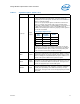
SLP# Input
SLP# (Sleep), when asserted in Stop-Grant state, causes the
processor to enter the Sleep state. During Sleep state, the
processor stops providing internal clock signals to all units, leaving
only the Phase-Locked Loop (PLL) still operating. Processors in this
state will not recognize snoops or interrupts. The processor will
recognize only assertion of the RESET# signal, deassertion of SLP#,
and removal of the BCLK input while in Sleep state. If SLP# is
deasserted, the processor exits Sleep state and returns to Stop-
Grant state, restarting its internal clock signals to the bus and
processor core units. If DPSLP# is asserted while in the Sleep state,
the processor will exit the Sleep state and transition to the Deep
Sleep state.
SMI# Input
SMI# (System Management Interrupt) is asserted asynchronously
by system logic. On accepting a System Management Interrupt, the
processor saves the current state and enter System Management
Mode (SMM). An SMI Acknowledge transaction is issued, and the
processor begins program execution from the SMM handler.
If SMI# is asserted during the deassertion of RESET# the processor
will tristate its outputs.
STPCLK# Input
STPCLK# (Stop Clock), when asserted, causes the processor to
enter a low power Stop-Grant state. The processor issues a Stop-
Grant Acknowledge transaction, and stops providing internal clock
signals to all processor core units except the FSB and APIC units.
The processor continues to snoop bus transactions and service
interrupts while in Stop-Grant state. When STPCLK# is deasserted,
the processor restarts its internal clock to all units and resumes
execution. The assertion of STPCLK# has no effect on the bus
clock; STPCLK# is an asynchronous input.
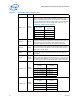
TCK Input
TCK (Test Clock) provides the clock input for the processor Test Bus
(also known as the Test Access Port).
Please contact your Intel representative for termination
requirements and implementation details.
TDI Input
TDI (Test Data In) transfers serial test data into the processor. TDI
provides the serial input needed for JTAG specification support.
Please contact your Intel representative for termination
requirements and implementation details.
TDO Output
TDO (Test Data Out) transfers serial test data out of the processor.
TDO provides the serial output needed for JTAG specification
support.
Please contact your Intel representative for termination
requirements and implementation details.
TEST1 Input
TEST1 must have a stuffing option of separate pull-down resistor to
V
SS
.
Please contact your Intel representative for more detailed
information.
TEST2 Input
TEST2 must have a 51 Ω ±5% pull-down resistor to V
SS
. Please
contact your Intel representative for more details.
THERMDA Other Thermal Diode Anode.
THERMDC Other Thermal Diode Cathode.
Table 17. Signal Description (Sheet 8 of 9)
Name Type Description