
Intel Core Duo Processor and Intel Core Solo Processor on 65 nm Process


Package Mechanical Specifications and Pin Information
62 Datasheet
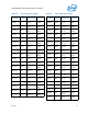
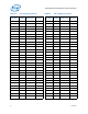
DINV[1]# M26
Source
Synch
Input/
Output
DINV[2]# V23
Source
Synch
Input/
Output
DINV[3]# AC20
Source
Synch
Input/
Output
DPRSTP# E5 CMOS Input
DPSLP# B5 CMOS Input
DPWR# D24
Common
Clock
Input
DRDY# F21
Common
Clock
Input/
Output
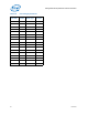
DSTBN[0]
#
H23
Source
Synch
Input/
Output
DSTBN[1]
#
M24
Source
Synch
Input/
Output
DSTBN[2]
#
W24
Source
Synch
Input/
Output
DSTBN[3]
#
AD23
Source
Synch
Input/
Output
DSTBP[0]
#
G22
Source
Synch
Input/
Output
DSTBP[1]
#
N25
Source
Synch
Input/
Output
DSTBP[2]
#
Y25
Source
Synch
Input/
Output
DSTBP[3]
#
AE24
Source
Synch
Input/
Output
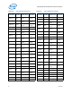
FERR# A5 Open Drain Output
GTLREF AD26 Power/Other Input
HIT# G6
Common
Clock
Input/
Output
HITM# E4
Common
Clock
Input/
Output
IERR# D20 Open Drain Output
IGNNE# C4 CMOS Input
INIT# B3 CMOS Input
Table 18. Pin Listing by Pin Name
Pin Name
Pin
Number
Signal
Buffer Type
Direction
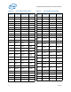
LINT0 C6 CMOS Input
LINT1 B4 CMOS Input
LOCK# H4
Common
Clock
Input/
Output
PRDY# AC2
Common
Clock
Output
PREQ# AC1
Common
Clock
Input
PROCHOT
#
D21 Open Drain
Input/
Output
PSI# AE6 CMOS Output
PWRGOOD D6 CMOS Input
REQ[0]# K3
Source
Synch
Input/
Output
REQ[1]# H2
Source
Synch
Input/
Output
REQ[2]# K2
Source
Synch
Input/
Output
REQ[3]# J3
Source
Synch
Input/
Output
REQ[4]# L5
Source
Synch
Input/
Output
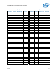
RESET# B1
Common
Clock
Input
RS[0]# F3
Common
Clock
Input
RS[1]# F4
Common
Clock
Input
RS[2]# G3
Common
Clock
Input
RSVD D2 Reserved
RSVD F6 Reserved
RSVD D3 Reserved
RSVD C1 Reserved
RSVD AF1 Reserved
RSVD D22 Reserved
Table 18. Pin Listing by Pin Name
Pin Name
Pin
Number
Signal
Buffer Type
Direction