SYS7180VE PICMG Single Board Computer For socket 478 CPU With VGA/ LAN (Pentium 4™&Celeron™& Intel® Celeron®DTM CPU) User’s Manual
Copyright This document is copyrighted, © 2004. All rights are reserved. The original manufacturer reserves the right to make improvements to the products described in this manual at any time without notice. No part of this manual may be reproduced, copied, translated or transmitted in any form or by any means without the prior written permission of the original manufacturer. Information provided in this manual is intended to be accurate and reliable.
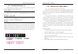
Table of Contents Table of Contents 2.5.10 2.5.11 2.5.12 2.5.13 Table of Contents CHAPTER 1 INTRODUCTION ...............................................1 1.1 1.2 1.3 1.4 SPECIFICATION ....................................................................1 CHECK LIST ........................................................................1 DESCRIPTION ......................................................................2 POWER REQUIREMENTS ......................................................2 1.
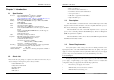
CHAPTER 1 – Introduction CHAPTER 1 – Introduction PS/2 1 to 2 adapter *1 Com extension cables with bracket *1 Com, Printer extension cables with bracket *1 +12V power cable *1 Chapter 1 Introduction 1.1 Specification Support Intel® PentiumTM 4 CPU up to 3.06 GHz Support Intel® CeleronTM CPU up to 2.60 GHz Support Intel® Celeron®DTM CPU up to 2.
CHAPTER 1 – Introduction CHAPTER 1 – Introduction 3.3 V output must reach its minimum regulation level within 20ms of the +5V 1.5 output reaching its minimum regulation level Connector & Jumper Location The following table lists the power supply’s tolerances for DC voltages: DC Voltage +3.
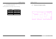
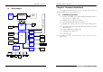
CHAPTER 1 – Introduction 1.6 CHAPTER 2 –Hardware Installations Chapter 2 Hardware Installations Block Diagram This chapter provides information on how to use the jumpers and connectors on the SYS7180VE in order to set up a workable system. DATA CTRL ADDR DDR266 Modules FCBGA760 PICMG PCI/ISA SLOT DATA CTRL ADDR DDR 266 Mhz BROOKDALE-G VGA CRT CONNECTOR Installation procedure 2.1.1 Insert the system BIOS (if not already installed) genteelly.
CHAPTER 2 –Hardware Installations 2.2 CHAPTER 2 –Hardware Installations CPU Installation: 2.3 The SYS7180VE Industrial CPU Card supports a single Intel® P4 CeleronTM or Celeron DTM processor and Pentium 4TM processor. The processor’s VID pins automatically program the voltage regulator on the CPU card to the required processor The SYS7180VE Industrial CPU Card supports two single-side or double-sided DDR266/333 unregistered, DIMM 184-pin sockets for a maximum total memory of 1GB.
CHAPTER 2 –Hardware Installations CHAPTER 2 –Hardware Installations Chipset 2.4 Jumper Settings: Intel 82845GV GMCH overview The features: Jumper 400/533 MHz PSB (100/133MHz bus clock) Jumper setting Default setting 32-bit addressing for access to 2GB of memory space up to 2GB of 266MHz FSB FSB setting: auto Short 1-2 or 333 MHz DDR SDRAM. JCC Clear CMOS: Normal mode Short 2-3 Supports only for un-buffered non-ECC DIMMs. JAV J4 Hub Interface: - Supports Hub Interface 1.
CHAPTER 2 –Hardware Installations CHAPTER 2 –Hardware Installations 2.5 2.4.
CHAPTER 2 –Hardware Installations CHAPTER 2 –Hardware Installations 2.5.1 Front Panel Connector: J1 2.5.2 USB Connector: USB1-2 USB3-4 This header can be connected to a front panel power switch.
CHAPTER 2 –Hardware Installations CHAPTER 2 –Hardware Installations 2.5.4 Serial Port connector: COM1/COM2 COM1, COM2 are use in the 10-pins box-header, are onboard serial ports of the CPU card SYS7180VE. The following table shows the pin assignments of these connectors. 2.5.
CHAPTER 2 –Hardware Installations CHAPTER 2 –Hardware Installations 2.88 MB, 3.5-inch These connectors support the provided IDE hard disk ribbon cable. After connecting the single end to the board, connect the two plugs at the other end to your hard This connector supports the provided floppy drive ribbon cable. After connecting disk(s).
CHAPTER 2 –Hardware Installations CHAPTER 2 –Hardware Installations 2.5.9 External Keyboard/Mouse Connector: 2.5.8 Adapter connector for GIGA LAN: LAN2 There are two 5-pin connectors for external keyboard&mouse. This connector is for the GIGA LAN adapter that 10/100/1000 Base-TX RJ45 single port (1X1) tab-UP with LEDs integrated magnetics connector. The follow table shows the pin assignments of this connector. PIN No.
CHAPTER 2 –Hardware Installations CHAPTER 2 –Hardware Installations 2.5.13 ACPI Connector: J2 2.5.10 VGA Connector: When used with an ATX-compliant power supply that supports remote power on/off, the CPU card can turn off the system power through software control. It is a VGA CRT connector. The pin assignments are as follows: 5 1 6 10 15 11 PIN No. 1 3 5 7 9 11 13 15 Function Red Blue GND GND VCC N.C H-Sync DDC clock PIN No. 2 4 6 8 10 12 14 16 Function Green N.C GND GND GND DDC data V-Sync N.
CHAPTER 2 –Hardware Installations CHAPTER 3 - BIOS SETUP Chapter 3 BIOS Setup 3.1 Introduction This chapter discusses Award’s Setup program built into the FLASH ROM BIOS. The Setup program allows users to modify the basic system configuration. This special information is then stored in battery-backed RAM so that it retains the Setup information when the power is turned off. The rest of this chapter is intended to guide you through the process of configuring your system using Setup.
CHAPTER 3 - BIOS SETUP CHAPTER 3 - BIOS SETUP the PageUp and PageDown keys to change entries, press for help and press to These defaults have been carefully chosen by both Award and your systems manufacturer quit. The following table provides more detail about how to navigate in the Setup program to provide the absolute maximum performance and reliability. Even a seemingly small using the keyboard. change to the chipset setup has the potential for causing you to use the override.
CHAPTER 3 - BIOS SETUP CHAPTER 3 - BIOS SETUP Advanced Chipset Features Use this menu to change the values in the chipset registers and optimize your system's performance. Integrated Peripherals Use this menu to specify your settings for integrated peripherals. See section 6.6. for the details. Power Management Setup Use this menu to specify your settings for power management. PnP / PCI Configuration This entry appears if your system supports PnP / PCI.
CHAPTER 3 - BIOS SETUP Item Video Halt On Options EGA/VGA CGA 40 CGA 80 MONO All Errors No Errors All, but Keyboard All, but Diskette All, but Disk/Key Base Memory N/A Extended Memory N/A Total Memory N/A CHAPTER 3 - BIOS SETUP Description Item Landing zone Select the default video device Sector Select the situation in which you want the BIOS to stop the POST process and notify you Options Min = 0 Max = 65535 Min = 0 Max = 255 Description **** Number of sectors per track 3.
CHAPTER 3 - BIOS SETUP Disabled No warning message will appear when anything attempts to access the boot sector or hard disk partition table. Description Choice CHAPTER 3 - BIOS SETUP Description Choice Boot Up NumLock Status Toggle between On or Off to control the state of the NumLock key when the system boots. When toggled On, the numeric keypad generates numbers instead of controlling cursor operations.
CHAPTER 3 - BIOS SETUP Description CHAPTER 3 - BIOS SETUP 3.5 Advanced Chipset Features Setup Choice Typematic Delay (Msec) When the typematic rate setting is enabled, you can select a typematic delay (the delay before key strokes begin to repeat) of 250, 500, 750 or 1000 milliseconds. Security Option Select whether the password is required every time the system boots or only when you enter setup.
CHAPTER 3 - BIOS SETUP Description Choice Description CAS Latency Time When synchronous DRAM is installed, the number of clock cycles of CAS latency depends on the DRAM timing. Do not reset this field from the default value specified by the system designer. You can select CAS latency time in HCLK of 2/2 or 3/3. The system board designer should set the values in this field, depends on the DRAM installed specifications of the installed DRAM or the installed CPU.
CHAPTER 3 - BIOS SETUP Description Choice CHAPTER 3 - BIOS SETUP Description Delay Transaction The chipset has an embedded 32-bit posted write buffer to support delay transactions cycles. Select Enabled to support compliance with PCI specification version 2.1. Choice On chip Frame buffer size When Enabled, a fixed VGA frame buffer from A000h to BFFFh and a CPU-to-PCI write buffer are implemented. 3.
CHAPTER 3 - BIOS SETUP Description Choice CHAPTER 3 - BIOS SETUP Description On-Chip Primary PCI IDE IDE Secondary Master/Slave PIO The integrated peripheral controller contains an IDE interface with support for two IDE channels. Select Enabled to activate each channel separately. The four IDE PIO (Programmed Input/Output) fields let you set a PIO mode (0-4) for each of the four IDE devices that the onboard IDE interface supports. Modes 0 through 4 provide successively increased performance.
CHAPTER 3 - BIOS SETUP Description Choice CHAPTER 3 - BIOS SETUP Description Choice sector the drive can support. USB Keyboard Support Onboard FDC Controller Select Enabled if your system contains a Universal Serial Bus (USB) controller and you have a USB keyboard. Select Enabled if your system has a floppy disk controller (FDC) installed on the system board and you wish to use it. If you install and-in FDC or the system has no floppy drive, select Disabled in this field.
CHAPTER 3 - BIOS SETUP Description CHAPTER 3 - BIOS SETUP Choice Parallel Port Mode Selected an operating mode for the onboard parallel port. Select Compatible or extended unless you are certain both your hardware and software support EPP or ECP mode. PWRON After PWR-Fail Select a Power On status by the BIOS setup when power fail. 3.
CHAPTER 3 - BIOS SETUP Description Choice CHAPTER 3 - BIOS SETUP Description Choice HDD Power Down Video Off Method When enabled and after the set time of system inactivity, the hard disk drive will be powered down while all other devices remain active. Video Off In Suspend This determines the manner in which the monitor is blanked.
CHAPTER 3 - BIOS SETUP Description Choice CHAPTER 3 - BIOS SETUP Description Choice Reload Global Timer Events: When Enabled, an event occurring on each listed device restarts the global timer for Standby mode. Resume by Alarm When Enabled, your can set the date and time at which the RTC (real-time clock) alarm awakens the system from Suspend mode.
CHAPTER 3 - BIOS SETUP CHAPTER 3 - BIOS SETUP IRQ n Resources 3.8 PnP/PCI Configuration Setup This section describes configuring the PCI bus system. PCI, or Personal Computer Interconnect, is a system which allows I/O devices to operate at speeds nearing the speed the CPU itself uses when communicating with its own special components. This section covers some very technical items and it is strongly recommended that only experienced users should make any changes to the default settings.
CHAPTER 3 - BIOS SETUP CHAPTER 3 - BIOS SETUP 3.9 PC Health Status 3.11 Supervisor/User Password Setting You can set either supervisor or user password, or both of then. The differences between are: SUPERVISOR PASSWORD: can enter and change the options of the setup menus. USER PASSWORD: just can only enter but do not have the right to change the options of the setup menus. When you select this unction, the following message will appear at the center of the screen to assist you in creating a password.
CHAPTER 3 - BIOS SETUP CHAPTER 3 - BIOS SETUP CMOS checksum error Pressing on this item asks for confirmation: Checksum of CMOS is incorrect. This can indicate that CMOS has become corrupt. This Save to CMOS and EXIT (Y/N)? Y Pressing “Y” stores the selections made in the menus in CMOS – a special section of error may have been caused by a weak battery. Check the battery and replace if necessary. DISK BOOT failure memory that stays on after you turn your system off.
CHAPTER 3 - BIOS SETUP Note: When either of these errors appear, the system will boot in ISA mode, which allows you to run the EISA Configuration Utility. Error encountered initializing hard drive CHAPTER 3 - BIOS SETUP the memory map for your system to find and replace the bad memory chips. Memory size has changed since last BOOT Memory has been added or removed since the last boot. In EISA mode use Configuration Hard drive cannot be initialized.
CHAPTER 3 - BIOS SETUP The board installed is not responding to the ID request, or no board ID has been found in CHAPTER 3 - BIOS SETUP is also used for M/B burn in test. BIOS ROM checksum error - System halted the indicated slot. NOTE: When this error appears, the system will boot in ISA mode, which allows you to run the EISA Configuration Utility. The checksum of ROM address F0000H-FFFFFH is bad. Memory test fail BIOS reports the memory tests fail if the onboard memory is tested error.
CHAPTER 3 - BIOS SETUP APPENDIX CHAPTER 3 - BIOS SETUP NOTE: Because WIN NT,win2000,win2003,winXP are not effective by writing the port directly, so we must make lib file、driver or DLL first. Watch-Dog-Timer (WDT) Setting 一. Definition for SYS7180VE watchdog The watchdog timer can be adjusted by software setting from 1second to 239seconds or from 1 minute to 239 minutes. The I/O port is defined at address EFH. You can trigger/enable disable the timer by writing port EFH.