
Technical Product Specification


Intel® Server Chassis SC5650 TPS Power Sub-system
Revision 1.2
Intel order number E39531-004
99
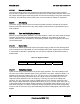
Table 116. Output Voltage Timing
Item Description Minimum Maximum Units
T
vout_rise
Output voltage rise time from each main output. 0.2* 20* msec
T
vout_on
All main outputs must be within regulation of each
other within this time.
50 msec
T
vout_off
All main outputs must leave regulation within this
time.
400 msec
* The 5VSB output voltage rise time should be from 0.2 ms to 25 ms.
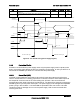
Figure 23. Output Voltage Timing
Table 117. Turn On / Off Timing
Item Description Minimum Maximum Units
T
sb_on_delay
Delay from AC being applied to 5VSB being within regulation.
1500
ms
T
ac_on_delay
Delay from AC being applied to all output voltages being within
regulation.
2500
ms
T
vout_holdup
Time all output voltages stay within regulation after loss of AC.
10
ms
T
pwok_holdup
Delay from loss of AC to de-assertion of PWOK
10
ms
T
pson_on_delay
Delay from PSON
#
active to output voltages within regulation limits.
5 400
ms
T
pson_pwok
Delay from PSON
#
deactivate to PWOK being de-asserted.
50
ms
T
pwok_on
Delay from output voltages within regulation limits to PWOK
asserted at turn on.
100 1000
ms
T
pwok_off
Delay from PWOK de-asserted to output voltages (3.3V, 5V, 12V, -
12V) dropping out of regulation limits.
1
ms
T
pwok_low
Duration of PWOK being in the de-asserted state during an off/on
cycle using AC or the PSON signal.
100
ms
Vout
10%
Vout
T
vout rise
T
vout_on
T
vout_off
V1
V2
V3
V4