
Technical Product Specification


Power Sub-system Intel® Server Chassis SC5650 TPS
Revision 1.2
Intel order number E39531-004
98
2.5.5.10 Common Mode Noise
The Common Mode noise on any output does not exceed 350mV pk-pk over the frequency
band of 10Hz to 20MHz.The measurement is made across a 100Ω resistor between each of the
DC outputs including ground at the DC power connector and chassis ground (power subsystem
enclosure). The test set-up uses an FET probe, such as a Tektronix* P6046, or equivalent.
2.5.5.11 Soft Starting
The Power Supply contains control circuit which provides monotonic soft start for its outputs
without overstress of the AC line or any power supply components at any specified AC line or
load conditions.
2.5.5.12 Zero Load Stability Requirements
When the power subsystem operates in a no load condition, it does not need to meet the output
regulation specification, but it operates without any tripping of over-voltage or other fault
circuitry. When the power subsystem is subsequently loaded, it begins to regulate and source
current without fault.
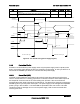
2.5.5.13 Ripple / Noise
The maximum allowed ripple/noise output of the power supply is defined in the following table.
This is measured over a bandwidth of 10 Hz to 20 MHz at the power supply output connectors.
A 10μF tantalum capacitor in parallel with a 0.1μF ceramic capacitor is placed at the point of
measurement.
Table 115. Ripple and Noise
+3.3V +5V +12V(1,2) -12V +5VSB
50mVp-p 50mVp-p 120mVp-p 120mVp-p 50mVp-p
2.5.5.14 Timing Requirements
These are the timing requirements for the power supply operation. The output voltages must
rise from 10% to within regulation limits (Tvout_rise) within 0.2 to 20ms, except for 5VSB - it is
allowed to rise from 0.2 to 25ms. The +3.3V, +5V and +12V1,+12V2 output voltages should
start to rise approximately at the same time. All outputs must rise monotonically. The 3.3V
output will not be greater than the +5V output by 1.5Vduring any point of the voltage rise
condition. The +5V output must never be greater than the +3.3V output by more than 2.25V.
Each output voltage shall reach regulation within 50ms (Tvout_on) of each other during turn on
of the power supply. Each output voltage shall fall out of regulation within 400ms (Tvout_off) of
each other during turn off. Table 21 shows the timing requirements for the power supply being
turned on and off via the AC input, with PSON held low and the PSON signal, with the AC input
applied