
Technical Product Specification


Intel® Server Chassis SC5600 Hot-swap Hard Disk Drive Bays
Revision 1.1
Intel order number E39532-004
55
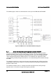
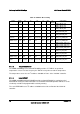
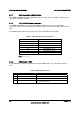
6.1.2 General Purpose Input/Output (GPIO)
The VSC410* controller supports customizable GPIO pins. The following table lists the GPIO
pins and their assigned functions.
Table 42. 6HDD VSC410* Controller GPIO Assignment
VSC410* Pin
Name
I/O
Type
Power
Well
Programming
Description
System Function Connection
P0_0 O 3.3 V
U3B1 FLASH ROM and U3C1
EEPROM write protect control
FM_EEPROM_WP Pull up 4.7 K to 3.3 V
P0_1 I 3.3 V IPMB Address allocation input SMB_3V3_IPMB_ADD Pull up 4.7 K to 3.3 V
P0_2 O 3.3 V HDD0 Fault LED control LED_DRV0_FLT_N Pull up 4.7 K to 3.3V
P0_3 I 3.3 V HDD0 Present detection FM_DRV0_PRSNT_N Pull up 4.7 K to 3.3 V
P0_4 O 3.3 V HDD1 Fault LED control LED_DRV1_FLT_N Pull up 4.7 K to 3.3 V
P0_5 I 3.3 V HDD1 Present detection FM_DRV1_PRSNT_N Pull up 4.7 K to 3.3 V
P0_6 O 3.3 V HDD2 Fault LED control LED_DRV2_FLT_N Pull up 4.7 K to 3.3 V
P0_7 I 3.3 V HDD2 Present detection FM_DRV2_PRSNT_N Pull up 4.7 K to 3.3 V
P1_0 O 3.3 V HDD3 Fault LED control LED_DRV3_FLT_N Pull up 4.7 K to 3.3 V
P1_1 I 3.3 V HDD3 Present detection FM_DRV3_PRSNT_N Pull up 4.7 K to 3.3 V
P1_2 O 3.3 V HDD4 Fault LED control LED_DRV4_FLT_N Pull up 4.7 K to 3.3 V
P1_3 I 3.3 V HDD4 Present detection FM_DRV4_PRSNT_N Pull up 4.7 K to 3.3 V
P1_4 O 3.3 V HDD5 Fault LED control LED_DRV5_FLT_N Pull up 4.7 K to 3.3 V
P1_5 I 3.3 V HDD5 Present detection FM_DRV5_PRSNT_N Pull up 4.7 K to 3.3 V
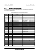
P1_6 O 3.3 V Test Point TP_LED_DRV6_FLT_N N/A
P1_7 O 3.3 V Test Point
TP_FM_DRV6_PRSNT_
N
N/A
P2_0 O 3.3 V Test Point TP_LED_DRV7_FLT_N N/A
P2_1 O 3.3 V Test Point
TP_FM_DRV7_PRSNT_
N
N/A
P2_2 O 3.3 V Test Point TP_LED_DRV8_FLT_N N/A
P2_3 O 3.3 V Test Point
TP_FM_DRV8_PRSNT_
N
N/A
P2_4 O 3.3 V Test Point TP_LED_DRV9_FLT_N N/A
P2_5 O 3.3 V Test Point
TP_FM_DRV9_PRSNT_
N
N/A
P2_6 O 3.3 V Test Point
TP_LED_DRV10_FLT_
N
N/A
P2_7 O 3.3 V Test Point
TP_FM_DRV10_PRSNT
_N
N/A
P3_0 I/O 3.3 V Clock signal of SGPIO interface SGPIO_CLK N/A
P3_1 I/O 3.3 V. Load signal of SGPIO interface SGPIO_LOAD N/A
P3_2 I/O 3.3 V SDATAIN signal of SGPIO interface SGPIO_DATAOUT0 N/A
P3_3 I/O 3.3 V
SDATAOUT signal of SGPIO
interface
SGPIO_DATAOUT1 N/A