
Technical Product Specification


Hot Swap Hard Disk Drive Bays Intel® Server Chassis SC5400 5U Kit TPS
68 Revision: 1.0
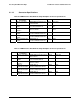
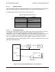
6.2.2 General Purpose Input/Output (GPIO)
The VSC7161* SAS Expander supports GPIO pins that are customizable. The following table
lists the GPIO pins with their assigned functions.
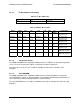
Table 55. VSC7161* SAS Expander GPIO Assignment
VSC7161*
PIN Name
I/O
Type
Power
Well
Programming
Description
System Function Reset
State
Initial
Value
Connection
P0_0 O 3.3V HDD0 Fault LED control LED_DRV0_FLT_N Pull up 4.7K to
3.3V
P0_1 O 3.3V HDD1 Fault LED control LED_DRV1_FLT_N Pull up 4.7K to
3.3V
P0_2 O 3.3V HDD2 Fault LED control LED_DRV2_FLT_N Pull up 4.7K to
3.3V
P0_3 O 3.3V HDD3 Fault LED control LED_DRV3_FLT_N Pull up 4.7K to
3.3V
P0_4 O 3.3V HDD4 Fault LED control LED_DRV4_FLT_N Pull up 4.7K to
3.3V
P0_5 O 3.3V HDD5 Fault LED control LED_DRV5_FLT_N Pull up 4.7K to
3.3V
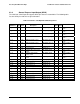
P0_6 O 3.3V Test Point P0_6 TP_EP_P0_6
P0_7 O 3.3V Test Point P0_7 TP_EP_P0_7
P0_8 O 3.3V FLASH(U3B1) write protect
control
FM_ROM0_WP_N Pull up 4.7K to
3.3V
P0_9 O 3.3V U3B2(not stuffed) write
protect control
FM_ROM1_WP_N Pull up 4.7K to
3.3V
P0_10 O 3.3V FRU(U3E2) write protect
control
FM_FRU_WP Pull up 4.7K to
3.3V
P0_11 O 3.3V Test Point P0_11 TP_EP_P0_11
P0_12 OI 3.3V Test Point P0_12 TP_EP_P0_12
P0_13 OI 3.3V Test Point P0_13 TP_EP_P0_13
P0_14 OI 3.3V Test Point P0_14 TP_EP_P0_14
P0_15 OI 3.3V Test Point P0_15 TP_EP_P0_15
P0_16 I 3.3V IPMB Address allocation input SMB_IPMB_ADDR Pull up 4.7K to
3.3V
P0_17 OI 3.3V Test Point P0_17 TP_EP_P0_17
P0_18 O 3.3V Test Point P0_18 TP_EP_P0_18
P0_19 OI 3.3V Test Point P0_19 TP_EP_P0_19
P0_22 O 3.3V Test Point P0_22 TP_EP_P0_22
P0_23 O 3.3V Test Point P0_23 TP_EP_P0_23