
Technical Product Specification


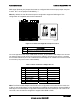
Table Of Contents
- 1. Introduction
- 2. Product Overview
- 3. Functional Architecture
- 3.1 Processor Support
- 3.1.1 Processor Population Rules
- 3.1.2 Multiple Processor Initialization
- 3.1.3 Enhanced Intel SpeedStep® Technology
- 3.1.4 Intel® Extended Memory 64 Technology (Intel® EM64T)
- 3.1.5 Execute Disable Bit Feature
- 3.1.6 Multi-Core Processor Support
- 3.1.7 Intel® Virtualization Technology
- 3.1.8 Platform Environmental Control Interface (PECI)
- 3.1.9 Common Enabling Kit (CEK) Design Support
- 3.2 Intel® 5400 Memory Controller Hub Chipset (Intel® 5400 MCH Chipset)
- 3.2.1 Processor Front-Side Buses
- 3.2.2 Snoop Filter
- 3.2.3 System Memory Controller and Memory Subsystem
- 3.2.3.1 Supported Memory
- 3.2.3.2 DIMM Population Rules and Supported DIMM Configurations
- 3.2.3.3 Minimum Memory Configuration
- 3.2.3.4 Memory upgrades
- 3.2.3.5 ECC Code Support
- 3.2.3.6 Memory Sparing
- 3.2.3.7 FBD Memory Thermal Management
- 3.2.3.8 BIOS Support of Memory Subsystem
- 3.2.3.9 Memory Error Handing
- 3.2.3.10 Memory Error Reporting
- 3.3 Intel® 6321ESB I/O Controller Hub
- 3.4 PCI Subsystem
- 3.4.1 Intel® 6321ESB I/O Controller Hub PCI32: 32-bit, 33-MHz PCI Bus Segment
- 3.4.2 Intel® 6321ESB I/O Controller Hub Port 1: x4 PCI Express* Bus Segment
- 3.4.3 Intel® 6321ESB I/O Controller Hub Port 2: x4 PCI Express* Bus Segment
- 3.4.4 MCH to Intel® 6321ESB I/O Controller Hub Chip-to-Chip Interface: Two x4 PCI Express* Bus Segments
- 3.4.5 MCH Ports 5-8: x16 Gen 2 PCI Express* Bus Segment
- 3.4.6 Scan Order
- 3.4.7 Resource Assignment
- 3.4.8 Automatic IRQ Assignment
- 3.4.9 Legacy Option ROM Support
- 3.4.10 EFI PCI APIs
- 3.4.11 Legacy PCI APIs
- 3.5 Video Support
- 3.6 Network Interface Controller (NIC)
- 3.7 Super I/O
- 3.1 Processor Support
- 4. Server Management
- 4.1 Intel® 6321ESB I/O Controller Hub Integrated Baseboard Management Controller (Integrated BMC) Feature Set
- 4.2 Advanced Configuration and Power Interface (ACPI)
- 4.3 System Initialization
- 4.4 Integrated Front Panel User Interface
- 4.5 Platform Control
- 4.6 Standard Fan Management
- 4.7 Private Management I2C Buses
- 4.8 Integrated BMC Messaging Interfaces
- 4.9 Event Filtering and Alerting
- 4.10 Watchdog Timer
- 4.11 System Event Log (SEL)
- 4.12 Sensor Data Record (SDR) Repository
- 4.13 Field Replaceable Unit (FRU) Inventory Device
- 4.14 Non-maskable Interrupt (NMI)
- 4.15 General Sensor Behavior
- 4.16 Processor Sensors
- 4.16.1 Processor Status Sensors
- 4.16.2 Processor VRD Over-temperature Sensor
- 4.16.3 ThermalTrip Monitoring
- 4.16.4 Internal Error (IERR) Monitoring
- 4.16.5 Dynamic Processor Voltage Monitoring
- 4.16.6 Processor Temperature Monitoring
- 4.16.7 Processor Thermal Control Monitoring (ProcHot)
- 4.16.8 CPU Population Error Sensor
- 4.17 Intel® Remote Management Module 2 (Intel RMM2) Support
- 5. System BIOS
- 5.1 BIOS Identification String
- 5.2 BIOS User Interface
- 5.2.1 Logo/Diagnostic Screen
- 5.2.2 BIOS Setup Utility
- 5.2.3 Server Platform Setup Utility Screens
- 5.2.3.1 Main Screen
- 5.2.3.2 Advanced Screen
- 5.2.3.3 Security Screen
- 5.2.3.4 Server Management Screen
- 5.2.3.5 Server Management System Information Screen
- 5.2.3.6 Boot Options Screen
- 5.2.3.7 Boot Manager Screen
- 5.2.3.8 Error Manager Screen
- 5.2.3.9 Exit Screen
- 5.3 Loading BIOS Defaults
- 5.4 Rolling BIOS
- 5.5 OEM Binary
- 6. Connector/Header Locations and Pin-outs
- 7. Jumper Block Settings
- 8. Intel® Light-Guided Diagnostics
- 9. Power and Environmental Specifications
- 9.1 Intel® Server Board S5400SF Design Specifications
- 9.2 Server Board Power Requirements
- 9.2.1 Processor Power Support
- 9.2.2 Power Supply DC Output Requirements
- 9.2.3 Power-on Loading
- 9.2.4 Grounding
- 9.2.5 Standby Outputs
- 9.2.6 Remote Sense
- 9.2.7 Voltage Regulation
- 9.2.8 Dynamic Loading
- 9.2.9 Capacitive Loading
- 9.2.10 Closed-Loop Stability
- 9.2.11 Common Mode Noise
- 9.2.12 Ripple/Noise
- 9.2.13 Soft Starting
- 9.2.14 Timing Requirements
- 9.2.15 Residual Voltage Immunity in Standby Mode
- 10. Regulatory and Certification Information
- Appendix A: Integration and Usage Tips
- Appendix B: POST Code Diagnostic LED Decoder
- Appendix C: POST Error Messages and Handling
- Appendix D: EFI Shell Commands
- Appendix E: Supported Intel® Server Chassis
- Appendix F: 1U PCI Express* Gen 2 Riser Card
- Glossary
- Reference Documents

Intel
®
Server Board S5400SF TPS Functional Architecture
Revision 2.02
Intel order number: D92944-007
39
3.4.4 MCH to Intel
®
6321ESB I/O Controller Hub Chip-to-Chip Interface: Two x4 PCI
Express* Bus Segments
The Enterprise Southbridge Interface (ESI) in the MCH is the chip-to-chip connection to the
Intel
®
6321ESB I/O Controller Hub. The ESI is a specialized inter-chip interface based upon the
PCI Express* Base Specification, Revision 1.1 with special commands/features added to
enhance the PCI Express* interface for enterprise applications. This high-speed interface
integrates advanced priority-based
servicing allowing for concurrent traffic. Base functionality is
completely transparent permitting current and legacy software to operate normally.
On the Intel
®
Server Board S5400SF, the ESI port in the MCH is combined with PCI Express*
Port 9 to augment the available bandwidth to the Intel
®
6321ESB I/O Controller Hub. When
operating alone, the available bi-directional bandwidth to the Intel
®
6321ESB I/O Controller Hub
is 2 GB/s (1 GB/s in each direction). When the ESI is paired with an additional x4 PCI Express*
link, the available bi-directional bandwidth to the Intel
®
6321ESB I/O Controller Hub is increased
to 4 GB/s.
3.4.5 MCH Ports 5-8: x16 Gen 2 PCI Express* Bus Segment
This PCI Express* bus segment combines four MCH x4 PCI Express* ports to support a high-
speed x16 Gen 2 interface for the on-board riser slot capable of supporting a maximum
theoretical bandwidth of 16 GB/s. The raw bit-rate per PCI Express* Gen 2 bit lane is 5 Gbit/s
with a maximum theoretical realized bandwidth of 2 GB/s in each direction.
3.4.5.1 PCI Express* Riser Slot
The server board has one 164-pin Gen 2 PCI Express* riser slot. See
Table 62 for the connector
pin-out definition.
Note: See Appendix F for a mechanical drawing showing the dimensional data for a 1U x16 PCI
Express* Gen 2 riser card as used in the Intel
®
Server System SR1560SF.
3.4.6 Scan Order
The BIOS assigns PCI bus numbers in a depth-first hierarchy, in accordance with the PCI Local
Bus Specification, Revision 2.2. The bus number is incremented when the BIOS encounters a
PCI-PCI bridge device. Scanning continues on the secondary side of the bridge until all
subordinate buses are assigned numbers. PCI bus number assignments may vary from boot to
boot with varying presence of PCI devices with PCI-PCI bridges. If a device with a bridge with a
single bus behind it is inserted into a PCI bus, all subsequent PCI bus numbers below the
current bus are increased by one.
The bus assignments occur once, early in the BIOS boot process, and never change during the
pre-boot phase.
3.4.7 Resource Assignment
The BIOS resource manager assigns the PIC-mode interrupt for the devices that are accessed
by the legacy code. The BIOS ensures the PCI BAR registers and the command registers for all
devices are correctly set up to match the behavior of the legacy BIOS after booting to a legacy
operating system. Any legacy code cannot make any assumption about the scan order of
devices or the order in which resources are allocated to them.