
Technical Product Specification


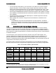

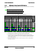
Table Of Contents
- 1. Introduction
- 2. Product Overview
- 3. Functional Architecture
- 3.1 Processor Support
- 3.1.1 Processor Population Rules
- 3.1.2 Multiple Processor Initialization
- 3.1.3 Enhanced Intel SpeedStep® Technology
- 3.1.4 Intel® Extended Memory 64 Technology (Intel® EM64T)
- 3.1.5 Execute Disable Bit Feature
- 3.1.6 Multi-Core Processor Support
- 3.1.7 Intel® Virtualization Technology
- 3.1.8 Platform Environmental Control Interface (PECI)
- 3.1.9 Common Enabling Kit (CEK) Design Support
- 3.2 Intel® 5400 Memory Controller Hub Chipset (Intel® 5400 MCH Chipset)
- 3.2.1 Processor Front-Side Buses
- 3.2.2 Snoop Filter
- 3.2.3 System Memory Controller and Memory Subsystem
- 3.2.3.1 Supported Memory
- 3.2.3.2 DIMM Population Rules and Supported DIMM Configurations
- 3.2.3.3 Minimum Memory Configuration
- 3.2.3.4 Memory upgrades
- 3.2.3.5 ECC Code Support
- 3.2.3.6 Memory Sparing
- 3.2.3.7 FBD Memory Thermal Management
- 3.2.3.8 BIOS Support of Memory Subsystem
- 3.2.3.9 Memory Error Handing
- 3.2.3.10 Memory Error Reporting
- 3.3 Intel® 6321ESB I/O Controller Hub
- 3.4 PCI Subsystem
- 3.4.1 Intel® 6321ESB I/O Controller Hub PCI32: 32-bit, 33-MHz PCI Bus Segment
- 3.4.2 Intel® 6321ESB I/O Controller Hub Port 1: x4 PCI Express* Bus Segment
- 3.4.3 Intel® 6321ESB I/O Controller Hub Port 2: x4 PCI Express* Bus Segment
- 3.4.4 MCH to Intel® 6321ESB I/O Controller Hub Chip-to-Chip Interface: Two x4 PCI Express* Bus Segments
- 3.4.5 MCH Ports 5-8: x16 Gen 2 PCI Express* Bus Segment
- 3.4.6 Scan Order
- 3.4.7 Resource Assignment
- 3.4.8 Automatic IRQ Assignment
- 3.4.9 Legacy Option ROM Support
- 3.4.10 EFI PCI APIs
- 3.4.11 Legacy PCI APIs
- 3.5 Video Support
- 3.6 Network Interface Controller (NIC)
- 3.7 Super I/O
- 3.1 Processor Support
- 4. Server Management
- 4.1 Intel® 6321ESB I/O Controller Hub Integrated Baseboard Management Controller (Integrated BMC) Feature Set
- 4.2 Advanced Configuration and Power Interface (ACPI)
- 4.3 System Initialization
- 4.4 Integrated Front Panel User Interface
- 4.5 Platform Control
- 4.6 Standard Fan Management
- 4.7 Private Management I2C Buses
- 4.8 Integrated BMC Messaging Interfaces
- 4.9 Event Filtering and Alerting
- 4.10 Watchdog Timer
- 4.11 System Event Log (SEL)
- 4.12 Sensor Data Record (SDR) Repository
- 4.13 Field Replaceable Unit (FRU) Inventory Device
- 4.14 Non-maskable Interrupt (NMI)
- 4.15 General Sensor Behavior
- 4.16 Processor Sensors
- 4.16.1 Processor Status Sensors
- 4.16.2 Processor VRD Over-temperature Sensor
- 4.16.3 ThermalTrip Monitoring
- 4.16.4 Internal Error (IERR) Monitoring
- 4.16.5 Dynamic Processor Voltage Monitoring
- 4.16.6 Processor Temperature Monitoring
- 4.16.7 Processor Thermal Control Monitoring (ProcHot)
- 4.16.8 CPU Population Error Sensor
- 4.17 Intel® Remote Management Module 2 (Intel RMM2) Support
- 5. System BIOS
- 5.1 BIOS Identification String
- 5.2 BIOS User Interface
- 5.2.1 Logo/Diagnostic Screen
- 5.2.2 BIOS Setup Utility
- 5.2.3 Server Platform Setup Utility Screens
- 5.2.3.1 Main Screen
- 5.2.3.2 Advanced Screen
- 5.2.3.3 Security Screen
- 5.2.3.4 Server Management Screen
- 5.2.3.5 Server Management System Information Screen
- 5.2.3.6 Boot Options Screen
- 5.2.3.7 Boot Manager Screen
- 5.2.3.8 Error Manager Screen
- 5.2.3.9 Exit Screen
- 5.3 Loading BIOS Defaults
- 5.4 Rolling BIOS
- 5.5 OEM Binary
- 6. Connector/Header Locations and Pin-outs
- 7. Jumper Block Settings
- 8. Intel® Light-Guided Diagnostics
- 9. Power and Environmental Specifications
- 9.1 Intel® Server Board S5400SF Design Specifications
- 9.2 Server Board Power Requirements
- 9.2.1 Processor Power Support
- 9.2.2 Power Supply DC Output Requirements
- 9.2.3 Power-on Loading
- 9.2.4 Grounding
- 9.2.5 Standby Outputs
- 9.2.6 Remote Sense
- 9.2.7 Voltage Regulation
- 9.2.8 Dynamic Loading
- 9.2.9 Capacitive Loading
- 9.2.10 Closed-Loop Stability
- 9.2.11 Common Mode Noise
- 9.2.12 Ripple/Noise
- 9.2.13 Soft Starting
- 9.2.14 Timing Requirements
- 9.2.15 Residual Voltage Immunity in Standby Mode
- 10. Regulatory and Certification Information
- Appendix A: Integration and Usage Tips
- Appendix B: POST Code Diagnostic LED Decoder
- Appendix C: POST Error Messages and Handling
- Appendix D: EFI Shell Commands
- Appendix E: Supported Intel® Server Chassis
- Appendix F: 1U PCI Express* Gen 2 Riser Card
- Glossary
- Reference Documents

Functional Architecture Intel
®
Server Board S5400SF TPS
Revision 2.02
Intel order number: D92944-007
20
The Snoop Filter lookup latency is four SF-clocks or two MCH core clocks to support
single snoop stall in an idle condition (single request issued from either bus). If both
buses make requests simultaneously, the snoop-filter always selects bus 0 first. In such
a scenario, bus 0 request has one snoop-stall and bus 1 request has two snoop-stalls.
Active Way/Invalid/E/M/Pseudo-Random replacement algorithm with updates on lookups
and invalidates; Invalid/Pseudo-Random replacement algorithm with updates on lookups
and invalidates.
Tag entries support a 38-bit physical address space. The MCH supports an external
address space of 38 bits as well.
ECC coverage with correction of single bit errors and detection of double bit errors
(SEC-DED).
- Invalid/Random Array does not implement ECC or parity protection. A bit failure
results in the selection of the wrong victim entry and may have a minimal impact on
performance. However, the coherency engine resolves the conflict and guarantee
correctness.
3.2.3 System Memory Controller and Memory Subsystem
The MCH masters four fully buffered DIMM (FBDIMM) memory channels. The four memory
channels are organized in to two branches. Each branch is supported by a separate memory
controller. The two channels on each branch operate in lock step to increase FBD bandwidth. A
branch transfers 16 bytes of payload/frame on Southbound lanes and 32 bytes of payload/frame
on Northbound lanes.
The host frequency is the speed of the memory interface of the Intel
®
5400 Chipset. This
frequency determines the speed at which the chipset completes a memory transaction. The
gear ratio determines the relative speed between the processor interface and the memory
interface. The BIOS supports 667 MHz and 800 MHz FB-DIMMs, and automatically selects and
configures the host frequency and gear ratio.
The following table shows the theoretical peak bandwidth of the Front-Side Bus and Memory
Bus when the server board is configured with supported processor and memory configurations.
Table 6. Front-Side Bus and Memory Bus Bandwidth
FSB Clock (Quad
pumped)
FSB Transfer
Rate
FSB BW FBD Channel
Frequency
DRAM Clock DRAM Transfer
Rate
FBD BW per
Branch
266 MHz
(1066 MHz)
1066 MT/s 8 GB/s 3.2 GHz 266 MHz 533 MT/s 8.4 GB/s
4 GHz 333 MHz 667 MT/s 10.6 GB/s
333 MHz
(1333 MHz)
1333 MT/s 10.7 GB/s 3.2 GHz 266 MHz 533 MT/s 8.4 GB/s
4 GHz 333 MHz 667 MT/s 10.6 GB/s
400 MHz
(1600 MHz)
1600 MT/s 12.8 GB/s 3.2 GHz 266 MHz 533 MT/s 8.4 GB/s
4 GHz 320 MHz
640 MT/s
1
10.2 GB/s
4.8 GHz 400 MHz 800 MT/s 12.8 GB/s
1
In system configurations that utilize processors supporting a 1600 MHz FSB and 667 MHz FBDIMMs concurrently,
the actual DRAM transer rate is 640 MT/s due to a set gear ratio inside the MCH.